
Datasheet


ADP5065 Data Sheet
Rev. D | Page 8 of 40
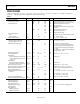
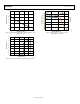
PIN CONFIGURATION AND FUNCTION DESCRIPTIONS
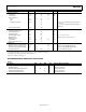
TOP VIEW
(BALL SIDE DOWN)
Not to Scale
1
A
B
C
D
E
2 3 4
BALL A1
CORNER
V_WEAK_SET
SDA
BAT_SNS
VIN1
THR
ISO_B1
ISO_S1
SW1
IIN_EXT
ISO_B2
ISO_S2
PGND1
SCL
TRK_EXT
AGND
SYS_ON_OK
VIN2 SW2 PGND2
CFILT
09370-003
Figure 3. Pin Configuration
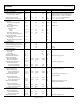
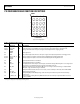
Table 6. Pin Function Descriptions
Pin
No. Mnemonic Type
1
Description
D3, E3 SW1, SW2 I/O DC-to-DC Converter Inductor Connection. These pins are high current outputs when in charging mode.
D1, E1 VIN1, VIN2 I/O Power Connection to USB VBUS. These pins are high current inputs when in charging mode.
D4, E4 PGND1,
PGND2
G Charger Power Ground. These pins are high current inputs when in charging mode.
C2 AGND G Analog Ground.
E2 CFILT I/O 4.7 μF Filter Capacitor Connection. This pin is a high current input/output when in charging mode.
C3, C4 ISO_S1, ISO_S2 I/O Charger Supply Side Input to Internal Isolation FET/Battery Current Regulation FET.
B3, B4 ISO_B1,
ISO_B2
I/O Battery Supply Side Input to Internal Isolation FET/Battery Current Regulation FET.
A2 SCL I I
2
C-Compatible Interface Serial Clock.
B1
SDA
I/O
I
2
C-Compatible Interface Serial Data.
A4 IIN_EXT I Set Input Current Limit. This pin sets the input current limit directly. When IIN_EXT = low or high-Z, the
input limit is 100 mA. When IIN_EXT = high, the input limit is 500 mA.
B2 TRK_EXT I Enable Trickle Charge Function. When TRK_EXT = low or high-Z, the trickle charge is enabled. When
TRK_EXT = high, the trickle charge is disabled.
A3
THR
I
Battery Pack Thermistor Connection. If not used, connect a dummy 10 kΩ resistor from THR to GND.
C1 BAT_SNS I Battery Voltage Sense Pin.
D2 SYS_ON_OK O Battery Okay Open-Drain Output Flag. Active low. This pin enables the system when the battery
reaches V
WEAK
.
A1 V_WEAK_SET I/O External Resistor Setting Pin for V_WEAK threshold. The use of this pin is optional. When not in use,
connect to GND.
1
I is input, O is output, I/O is input/output, and G is ground.