
Datasheet

ADPD1080/ADPD1081 Data Sheet
Rev. B | Page 14 of 74
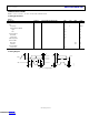
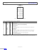
PIN CONFIGURATIONS AND FUNCTION DESCRIPTIONS
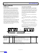
16110-006
1GPIO0
2GPIO1
3DVDD
4AGND
5VREF
6AVDD
7PD1
17 NIC
18 NIC
19 NIC
20 NIC
21 NIC
16 NIC
15 PD8
8PD2
9PD3
10PD4
11PDC
12PD5
13PD6
14PD7
24 LEDX3
25 LEDX2
26 LGND
27 SCL
28 SDA
23 LEDX1
22 NIC
ADPD1080
TOP VIEW
(Not to Scale)
NOTES
1. NIC = NOT INTERNALLY CONNECTED (NONBONDED PAD).
THIS PIN CAN BE GROUNDED.
2. EXPOSED PAD (DIGITAL GROUND). CONNECT THE
EXPOSED PAD TO GROUND.
Figure 6. 28-Lead LFCSP Pin Configuration (ADPD1080)
Table 12. 28-Lead LFCSP Pin Function Descriptions (ADPD1080)
Pin No. Mnemonic Type
1
Description
1 GPIO0 DIO General-Purpose Input/Output 0. This pin is used for interrupts and various clocking options.
2 GPIO1 DIO General-Purpose Input/Output 1. This pin is used for interrupts and various clocking options.
3 DVDD S 1.8 V Digital Supply.
4 AGND S Analog Ground.
5 VREF REF Internally Generated ADC Voltage Reference. Buffer this pin with a 1 µF capacitor to AGND.
6 AVDD S 1.8 V Analog Supply.
7 PD1 AI Photodiode Current Input (Anode) 1. If not in use, leave this pin floating.
8 PD2 AI Photodiode Current Input (Anode) 2. If not in use, leave this pin floating.
9 PD3 AI Photodiode Current Input (Anode) 3. If not in use, leave this pin floating.
10 PD4 AI Photodiode Current Input (Anode) 4. If not in use, leave this pin floating.
11 PDC AO Photodiode Common Cathode Bias.
12 PD5 AI Photodiode Current Input (Anode) 5. If not in use, leave this pin floating.
13 PD6 AI Photodiode Current Input (Anode) 6. If not in use, leave this pin floating.
14 PD7 AI Photodiode Current Input (Anode) 7. If not in use, leave this pin floating.
15 PD8 AI Photodiode Current Input (Anode) 8. If not in use, leave this pin floating.
16 to 22 NIC R Not Internally Connected (Nonbonded Pad). This pin can be grounded.
23 LEDX1 AO LED Driver 1 Current Sink. If not in use, leave this pin floating.
24 LEDX3 AO LED Driver 3 Current Sink. If not in use, leave this pin floating.
25 LEDX2 AO LED Driver 2 Current Sink. If not in use, leave this pin floating.
26 LGND S LED Driver Ground.
27 SCL DI I
2
C Clock Input.
28 SDA DIO I
2
C Data Input/Output.
EPAD (DGND) S Exposed Pad (Digital Ground). Connect the exposed pad to ground.
1
DIO means digital input/output, S means supply, REF means voltage reference, AI means analog input, AO means analog output, R means reserved, and DI means
digital input.
Downloaded from Arrow.com.Downloaded from Arrow.com.Downloaded from Arrow.com.Downloaded from Arrow.com.Downloaded from Arrow.com.Downloaded from Arrow.com.Downloaded from Arrow.com.Downloaded from Arrow.com.Downloaded from Arrow.com.Downloaded from Arrow.com.Downloaded from Arrow.com.Downloaded from Arrow.com.Downloaded from Arrow.com.Downloaded from Arrow.com.