
2/40-Bit IEEE Floating-Point DSP Microprocessor Specification Sheet
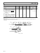
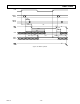

RECOMMENDED OPERATING CONDITIONS
K Grade B Grade T Grade
Parameter Min Max Min Max Min Max Unit
V
DD
Supply Voltage 4.50 5.50 4.50 5.50 4.50 5.50 V
T
AMB
Ambient Operating Temperature 0 +70 –40 +85 –55 +125 °C
Refer to Environmental Conditions for information on thermal specifications.
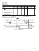
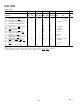
ELECTRICAL CHARACTERISTICS
Parameter Test Conditions Min Max Unit
V
IH
Hi-Level Input Voltage
1
V
DD
= max 2.0 V
V
IHCR
Hi-Level Input Voltage
2, 12
V
DD
= max 3.0 V
V
IL
Lo-Level Input Voltage
1, 12
V
DD
= min 0.8 V
V
ILC
Lo-Level Input Voltage
2
V
DD
= max 0.6 V
V
OH
Hi-Level Output Voltage
3, 11
V
DD
= min, I
OH
= –1.0 mA 2.4 V
V
OL
Lo-Level Output Voltage
3, 11
V
DD
= min, I
OL
= 4.0 mA 0.4 V
I
IH
Hi-Level Input Current
4, 5
V
DD
= max, V
IN
= V
DD
max 10 µA
I
IL
Lo-Level Input Current
4
V
DD
= max, V
IN
= 0 V 10 µA
I
ILT
Lo-Level Input Current
5
V
DD
= max, V
IN
= 0 V 350 µA
I
OZH
Tristate Leakage Current
6
V
DD
= max, V
IN
= V
DD
max 10 µA
I
OZL
Tristate Leakage Current
6
V
DD
= max, V
IN
= 0 V 10 µA
I
DDIN
Supply Current (Internal)
7
t
CK
= 30–33 ns, V
DD
= max, V
IHCR
= 3.0 V, 490 mA
V
IH
= 2.4 V, V
IL
= V
ILC
= 0.4 V
I
DDIDLE
Supply Current (Idle)
8
V
DD
= max, V
IN
= 0 V or V
DD
max 150 mA
C
IN
Input Capacitance
9, 10
f
IN
= 1 MHz, T
CASE
= 25°C, V
IN
= 2.5 V 10 pF
NOTES
l
Applies to: PMD47–0, PMACK, PMTS, DMD39–0, DMACK, DMTS, IRQ3–0. FLAG3–0, BR, TMS, TDI.
2
Applies to: CLKIN, TCK.
3
Applies to: PMA23–0, PMD47–0, PMS1–0, PMRD, PMWR, PMPAGE, DMA31–0, DMD39–0, DMS3–0, DMRD, DMWR, DMPAGE, FLAG3–0,
TIMEXP, BG.
4
Applies to: PMACK, PMTS, DMACK, DMTS, IRQ3–0, BR, CLKIN, RESET, TCK.
5
Applies to: TMS, TDI, TRST.
6
Applies to: PMA23–0, PMD47–0, PMS1–0, PMRD, PMWR, PMPAGE, DMA31–0, DMD39–0, DMS3–0, DMRD, DMWR, DMPAGE, FLAG3–0, TDO.
7
Applies to IVDD pins. At t
CK
= 30–33 ns, I
DDIN
(typical) = 230 mA; at t
CK
= 40 ns, I
DDIN
(max) = 420 mA and I
DDIN
(typical) = 200 mA; at t
CK
= 50 ns,
I
DDIN
(max) = 370 mA and I
DDIN
(typical) = 115 mA. See “Power Dissipation” for calculation of external (EVDD) supply current for total supply current.
8
Applies to IVDD pins. Idle refers to ADSP-21020 state of operation during execution of the IDLE instruction.
9
Guaranteed but not tested.
10
Applies to all signal pins.
11
Although specified for TTL outputs, all ADSP-21020 outputs are CMOS-compatible and will drive to V
DD
and GND assuming no dc loads.
12
Applies to RESET, TRST.
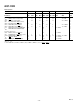
ABSOLUTE MAXIMUM RATINGS*
Supply Voltage . . . . . . . . . . . . . . . . . . . . . . . . . –0.3 V to +7 V
Input Voltage . . . . . . . . . . . . . . . . . . . . –0.3 V to V
DD
+ 0.3 V
Output Voltage Swing . . . . . . . . . . . . . –0.3 V to V
DD
+ 0.3 V
Load Capacitance . . . . . . . . . . . . . . . . . . . . . . . . . . . . 200 pF
Operating Temperature Range (Ambient) . . –55°C to +125°C
Storage Temperature Range . . . . . . . . . . . . –65°C to +150°C
Lead Temperature (10 seconds) CPGA . . . . . . . . . . . +300°C
ESD SENSITIVITY
The ADSP-21020 features proprietary input protection circuitry to dissipate high energy discharges
(Human Body Model). Per method 3015 of MIL-STD-883, the ADSP-21020 has been classified
as a Class 3 device, with the ability to withstand up to 4000 V ESD.
Proper ESD precautions are strongly recommended to avoid functional damage or performance
degradation. Charges readily accumulate on the human body and test equipment and discharge
without detection. Unused devices must be stored in conductive foam or shunts, and the foam
should be discharged to the destination socket before devices are removed. For further information
on ESD precautions, refer to Analog Devices’ ESD Prevention Manual.
*Stresses above those listed under “Absolute Maximum Ratings” may cause
permanent damage to the device. These are stress ratings only and functional
operation of the device at these or any other conditions above those indicated in the
operational sections of this specification is not implied. Exposure to absolute
maximum rating conditions for extended periods may affect device reliability.
REV. C
–12–
ADSP-21020–SPECIFICATIONS
WARNING!
ESD SENSITIVE DEVICE