
2/40-Bit IEEE Floating-Point DSP Microprocessor Specification Sheet

ADSP-21020
REV. C
–13–
TIMING PARAMETERS
General Notes
See Figure 15 on page 24 for voltage reference levels. Use the exact timing information given. Do not attempt to derive parameters
from the addition or subtraction of others. While addition or subtraction would yield meaningful results for an individual device, the
values given in this data sheet reflect statistical variations and worst cases. Consequently, you cannot meaningfully add parameters to
derive other specifications.
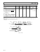
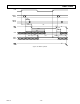
Clock Signal
K/B/T Grade K/B/T Grade B/T Grade K Grade
20 MHz 25 MHz 30 MHz 33.3 MHz
Parameter Min Max Min Max Min Max Min Max Unit
Timing Requirement:
t
CK
CLKIN Period 50 150 40 150 33 150 30 150 ns
t
CKH
CLKIN Width High 10 10 10 10 ns
t
CKL
CLKIN Width Low 10 10 10 10 ns
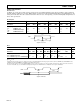
CLKIN
t
CKH
t
CKL
t
CK
Figure 3. Clock
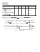
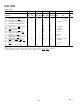
Reset
K/B/T Grade K/B/T Grade B/T Grade K Grade
20 MHz 25 MHz 30 MHz 33.3 MHz Frequency Dependency*
Parameter Min Max Min Max Min Max Min Max Min Max Unit
Timing Requirement:
t
WRST
1
RESET Width Low 200 160 132 120 4t
CK
ns
t
SRST
2
RESET Setup before CLKIN High 29 50 24 40 21 33 19 30 29 + DT/2 30 ns
NOTES
DT = t
CK
–50 ns
1
Applies after the power-up sequence is complete. At power up, the Internal Phase Locked Loop requires no more than 1000 CLKIN cycles while RESET is low,
assuming stable V
DD
and CLKIN (not including clock oscillator start-up time).
2
Specification only applies in cases where multiple ADSP-21020 processors are required to execute in program counter lock-step (all processors start execution at
location 8 in the same cycle). See the Hardware Configuration chapter of the ADSP-21020 User’s Manual for reset sequence information.
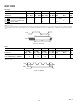
CLKIN
t
WRST
t
SRST
RESET
Figure 4. Reset