
2/40-Bit IEEE Floating-Point DSP Microprocessor Specification Sheet

ADSP-21020
REV. C
–25–
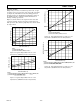
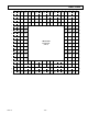
Capacitive Loading
Output delays are based on standard capacitive loads: 100 pF
on address, select, page and strobe pins, and 50 pF on all others
(see Figure 14). For different loads, these timing parameters
should be derated. See the Hardware Configuration chapter of
the ADSP-21020 User’s Manual for further information on
derating of timing specifications.
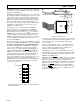
Figures 16 and 17 show how the output rise time varies with
capacitance. Figures 18 and 19 show how output delays vary
with capacitance. Note that the graphs may not be linear outside
the ranges shown.
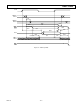
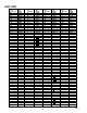
10
0
200
3
1
50
2
25
6
4
5
7
8
9
17515012510075
LOAD CAPACITANCE – pF
RISE TIME – ns (0.8V – 2.0V)
1
2
9.18
1.46
1.31
NOTES:
(1) OUTPUT PINS BG, TIMEXP
(2) OUTPUT PINS PMD47–0, DMD39–0, FLAG3–0
3.95
Figure 16. Typical Output Rise Time vs. Load
Capacitance (at Maximum Case Temperature)
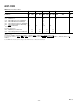
0
200
3
1
50
2
25
4
175
125
100
75 150
LOAD CAPACITANCE – pF
RISE TIME – ns (0.8V – 2.0V)
1
2
3.59
3.00
1.33
0.85
NOTES:
(1) OUTPUT PINS PMA23–0, PMS1–0, PMPAGE, DMA31–0, DMS3–0, DMPAGE, TDO
(2) OUTPUT PINS PMRD, PMWR, DMRD, DMWR
π
Figure 17. Typical Output Rise Time vs. Load
Capacitance (at Maximum Case Temperature)
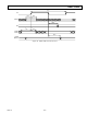
10
–2
200
4
NOMINAL
50
2
25
8
6
175
125
100
75 150
1
2
11.19
5.34
–1.86
– 0.89
LOAD CAPACITANCE – pF
OUTPUT DELAY OR HOLD – ns
NOTES:
(1) OUTPUT PINS BG, TIMEXP
(2) OUTPUT PINS PMD47–0, DMD39–0, FLAG3–0
12
Figure 18. Typical Output Delay or Hold vs. Load
Capacitance (at Maximum Case Temperature)
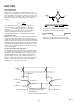
–3
200
NOMINAL
–2
50
–1
25
3
1
2
17515012510075
1
2
2.99
2.27
– 1.70
– 2.24
LOAD CAPACITANCE – pF
OUTPUT DELAY OR HOLD – ns
NOTES:
(1) OUTPUT PINS PMA23–0, PMS1–0, PMPAGE, DMA31–0, DMS3–0, DMPAGE, TDO
(2) OUTPUT PINS PMRD, PMWR, DMRD, DMWR
Figure 19. Typical Output Delay or Hold vs. Load
Capacitance (at Maximum Case Temperature)