
Datasheet


ADSP-21061/ADSP-21061L
Rev. D | Page 3 of 52 | May 2013
GENERAL DESCRIPTION
The ADSP-21061 SHARC—Super Harvard Architecture Com-
puter—is a signal processing microcomputer that offers new
capabilities and levels of performance. The ADSP-21061
SHARC is a 32-bit processor optimized for high performance
DSP applications. The ADSP-21061 builds on the ADSP-21000
DSP core to form a complete system-on-a-chip, adding a dual-
ported on-chip SRAM and integrated I/O peripherals supported
by a dedicated I/O bus.
Fabricated in a high speed, low power CMOS process, the
ADSP-21061 has a 20 ns instruction cycle time and operates at
50 MIPS. With its on-chip instruction cache, the processor can
execute every instruction in a single cycle. Table 1 shows perfor-
mance benchmarks for the ADSP-21061/ADSP-21061L.
The ADSP-21061 SHARC represents a new standard of integra-
tion for signal computers, combining a high performance
floating-point DSP core with integrated, on-chip system fea-
tures including 1M bit SRAM memory, a host processor
interface, a DMA controller, serial ports, and parallel bus con-
nectivity for glueless DSP multiprocessing.
The ADSP-21061 continues SHARC’s industry-leading stan-
dards of integration for DSPs, combining a high performance
32-bit DSP core with integrated, on-chip system features.
The block diagram on Page 1, illustrates the following architec-
tural features:
• Computation units (ALU, multiplier, and shifter) with a
shared data register file
• Data address generators (DAG1, DAG2)
• Program sequencer with instruction cache
• PM and DM buses capable of supporting four 32-bit data
transfers between memory and the core at every core pro-
cessor cycle
•Interval timer
•On-chip SRAM
• External port for interfacing to off-chip memory and
peripherals
• Host port and multiprocessor interface
• DMA controller
•Serial ports
• JTAG test access port
SHARC FAMILY CORE ARCHITECTURE
The ADSP-21061 includes the following architectural features
of the ADSP-21000 family core. The ADSP-21061 processors
are code- and function-compatible with the ADSP-21020,
ADSP-21060, and ADSP-21062 SHARC processors.
Independent, Parallel Computation Units
The arithmetic/logic unit (ALU), multiplier, and shifter all per-
form single-cycle instructions. The three units are arranged in
parallel, maximizing computational throughput. Single multi-
function instructions execute parallel ALU and multiplier oper-
ations. These computation units support IEEE 32-bit single-
precision floating-point, extended-precision 40-bit floating-
point, and 32-bit fixed-point data formats.
Data Register File
A general-purpose data register file is used for transferring data
between the computation units and the data buses, and for stor-
ing intermediate results. This 10-port, 32-register (16 primary,
16 secondary) register file, combined with the ADSP-21000
Harvard architecture, allows unconstrained data flow between
computation units and internal memory.
Table 1. Benchmarks (at 50 MHz)
Benchmark Algorithm Speed Cycles
1024 Point Complex FFT (Radix 4,
with reversal)
.37 ms 18,221
FIR Filter (per tap) 20 ns 1
IIR Filter (per biquad) 80 ns 4
Divide (y/x) 120 ns 6
Inverse Square Root 180 ns 9
DMA Transfer Rate 300M bps
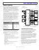
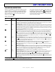
Figure 2. ADSP-21061/ADSP-21061L System Sample Configuration
3
4
RESET JTAG
7
ADSP-21061
BMS
1 ⫻ CLOCK
CS
BOOT
EPROM
(OPTIONAL)
MEMORY-
MAPPED
DEVICES
(OPTIONAL)
OE
DATA
DMA DEVICE
(OPT IONAL)
DATA
ADDR
DATA
HOST
PROCESSOR
INTERFACE
(OPTIONAL)
CS
RD
PAGE
ADRCLK
ACK
BR
1–6
DMAR
1–2
CLKIN
IRQ
2–0
TCLK0
RPBA
EBOOT
LBOOT
FLAG
3–0
TIMEXP
DR0
DT0
RSF0
TFS0
RCLK0
TCLK1
DR1
DT1
RSF1
TFS1
RCLK1
ID
2–0
SERIAL
DEVICE
(OPTIONAL)
SERIAL
DEVICE
(OPTIONAL)
CPA
REDY
HBG
HBR
DMAG
1–2
SBTS
MS
3–0
WR
DATA
47–0
DATA
ADDR
CS
ACK
WE
ADDR
31–0
D
A
T
A
C
O
N
T
R
O
L
A
D
D
R
E
S
S
ADDR
TO GND
SW