a Commercial Grade SHARC DSP Microcomputer ADSP-21061/ADSP-21061L SUMMARY High performance signal processor for communications, graphics, and imaging applications Super Harvard Architecture Four independent buses for dual data fetch, instruction fetch, and nonintrusive I/O 32-bit IEEE floating-point computation units—multiplier, ALU, and shifter Dual-ported on-chip SRAM and integrated I/O peripherals—a complete system-on-a-chip Integrated multiprocessing features KEY FEATURES—PROCESSOR CORE Dual data ad
ADSP-21061/ADSP-21061L TABLE OF CONTENTS Summary ............................................................... 1 ADSP-21061L Specifications ..................................... 17 Key Features—Processor Core ................................. 1 Operating Conditions (3.3 V) ................................. 17 General Description ................................................. 3 Electrical Characteristics (3.3 V) ............................. 17 SHARC Family Core Architecture ......................
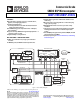
ADSP-21061/ADSP-21061L GENERAL DESCRIPTION ADSP-21061 1 ⫻ CLOCK TO GND CLKIN 3 4 CS BMS EBOOT ADDR LBOOT DATA FLAG3–0 ADDR31–0 ADDR TIMEXP DATA47–0 DATA MEMORYMAPPED OE DEVICES WE (OPTIONAL) ACK RD SERIAL DEVICE (OPTIONAL) SERIAL DEVICE (OPTIONAL) Table 1. Benchmarks (at 50 MHz) TCLK0 RCLK0 TFS0 RSF0 DT0 DR0 TCLK1 RCLK1 TFS1 RSF1 DT1 DR1 WR ACK CS MS3–0 PAGE SW SBTS ADRCLK DMAR1–2 Speed .
ADSP-21061/ADSP-21061L Single-Cycle Fetch of Instruction and Two Operands The ADSP-21061 features an enhanced Harvard architecture in which the data memory (DM) bus transfers data and the program memory (PM) bus transfers both instructions and data (Figure 1 on Page 1). With its separate program and data memory buses and on-chip instruction cache, the processor can simultaneously fetch two operands and an instruction (from the cache), all in a single cycle.
ADDRESS DATA DATA RESET ADDRESS ADSP-21061 #3 CLKIN CONTROL ADSP-21061 #6 ADSP-21061 #5 ADSP-21061 #4 CONTROL ADSP-21061/ADSP-21061L ADDR31–0 DATA47–0 RPBA 3 ID2–0 CONTROL 011 BR1–2, BR4–6 5 BR3 ADSP-21061 #2 CLKIN ADDR31–0 RESET DATA47–0 RPBA 3 ID2–0 CONTROL 010 CPA BR1, BR3–6 BR2 5 ADSP-21061 #1 CLKIN RESET ADDR DATA47–0 DATA RDx ID2–0 WRx ACK MS3–0 CONTROL RPBA 3 001 ADDR31–0 OE WE ACK CS BMS PAGE CS ADDR SBTS BUS PRIORITY RESET CLOCK GLOBAL MEMORY AND PERIPHERAL (OP
ADSP-21061/ADSP-21061L The serial ports can operate with little-endian or big-endian transmission formats, with word lengths selectable from 3 bits to 32 bits. They offer selectable synchronization and transmit modes as well as optional μ-law or A-law companding. Serial port clocks and frame syncs can be internally or externally generated. The serial ports also include keyword and key mask features to enhance interprocessor communication.
ADSP-21061/ADSP-21061L Program Booting The internal memory of the ADSP-21061 can be booted at system power-up from either an 8-bit EPROM, or a host processor. Selection of the boot source is controlled by the BMS (boot memory select), EBOOT (EPROM boot), and LBOOT (host boot) pins. 32-bit and 16-bit host processors can be used for booting. PORTING CODE FROM THE ADSP-21060 OR ADSP-21062 The ADSP-21061 is pin compatible with the ADSP-21060/ ADSP-21061/ADSP-21062 processors.
ADSP-21061/ADSP-21061L Board Support Packages for Evaluation Hardware RELATED SIGNAL CHAINS Software support for the EZ-KIT Lite evaluation boards and EZExtender daughter cards is provided by software add-ins called Board Support Packages (BSPs). The BSPs contain the required drivers, pertinent release notes, and select example code for the given evaluation hardware. A download link for a specific BSP is located on the web page for the associated EZ-KIT or EZExtender product.
ADSP-21061/ADSP-21061L PIN FUNCTION DESCRIPTIONS ADSP-21061 pin definitions are listed below. All pins are identical on the ADSP-21061 and ADSP-21061L. Inputs identified as synchronous (S) must meet timing requirements with respect to CLKIN (or with respect to TCK for TMS, TDI). Inputs identified as asynchronous (A) can be asserted asynchronously to CLKIN (or to TCK for TRST).
ADSP-21061/ADSP-21061L Table 2. Pin Descriptions (Continued) Pin ACK Type I/O/S Function Memory Acknowledge. External devices can deassert ACK (low) to add wait states to an external memory access. ACK is used by I/O devices, memory controllers, or other peripherals to hold off completion of an external memory access. The ADSP-21061 deasserts ACK as an output to add wait states to a synchronous access of its internal memory.
ADSP-21061/ADSP-21061L Table 2. Pin Descriptions (Continued) Pin TFSx RFSx EBOOT Type I/O I/O I LBOOT BMS I I/O/T* Function Transmit Frame Sync (Serial Ports 0, 1). Receive Frame Sync (Serial Ports 0, 1). EPROM Boot Select. When EBOOT is high, the ADSP-21061 is configured for booting from an 8-bit EPROM. When EBOOT is low, the LBOOT and BMS inputs determine booting mode. See the table in the BMS pin description below. This signal is a system configuration selection that should be hardwired. Link Boot.
ADSP-21061/ADSP-21061L TARGET BOARD CONNECTOR FOR EZ-ICE PROBE The ADSP-2106x EZ-ICE Emulator uses the IEEE 1149.1 JTAG test access port of the ADSP-2106x to monitor and control the target board processor during emulation. The EZ-ICE probe requires the ADSP-2106x’s CLKIN, TMS, TCK, TDI, TDO, and GND signals be made accessible on the target system via a 14-pin connector (a 2-row, 7-pin strip header) such as that shown in Figure 5.
ADSP-21061/ADSP-21061L OTHER JTAG CONTROLLER EM U TR S T TDO TDI TCK TRST TCK TDO TMS TDI T R ST TMS TDO EMU TDI TCK TDI EZ-ICE JTAG CONNECTOR ADSP-2106x n TMS JTAG DEVICE (OPTIONAL) ADSP-2106x #1 TCK TMS EMU TRST TDO CLKIN OPTIONAL Figure 6. JTAG Scan Path Connections for Multiple ADSP-2106x Systems * TDI EMU * TDI TDO TDI TDO TDI TDO TDI TDO TDI TDO TDI TDO 5k⍀ 5k⍀ TCK TMS TRST TDO CLKIN EMU *OPEN-DRAIN DRIVER OR EQUIVALENT, i.e, Figure 7.
ADSP-21061/ADSP-21061L ADSP-21061 SPECIFICATIONS OPERATING CONDITIONS (5 V) K Grade Parameter Description Min Nom Max Unit VDD Supply Voltage 4.75 5.0 5.25 V Case Operating Temperature 0 85 C VIH1 1 High Level Input Voltage @ VDD = Max 2.0 VDD + 0.5 V VIH2 2 High Level Input Voltage @ VDD = Max 2.2 VDD + 0.5 V Low Level Input Voltage @ VDD = Min –0.5 +0.
ADSP-21061/ADSP-21061L INTERNAL POWER DISSIPATION (5 V) These specifications apply to the internal power portion of VDD only. See the Power Dissipation section of this data sheet for calculation of external supply current and total supply current. For Operation Instruction Type Instruction Fetch Core Memory Access Internal Memory DMA a complete discussion of the code used to measure power dissipation, see the technical note “SHARC Power Dissipation Measurements.
ADSP-21061/ADSP-21061L EXTERNAL POWER DISSIPATION (5 V) Total power dissipation has two components, one due to internal circuitry and one due to the switching of external output drivers. Internal power dissipation is dependent on the instruction execution sequence and the data operands involved. Internal power dissipation is calculated in the following way: PINT = IDDIN VDD The load capacitance should include the processor’s package capacitance (CIN).
ADSP-21061/ADSP-21061L ADSP-21061L SPECIFICATIONS OPERATING CONDITIONS (3.3 V) A Grade K Grade Parameter Description Min Nom Max Min Nom Max Unit VDD Supply Voltage 3.15 3.3 3.45 3.15 3.3 3.45 V Case Operating Temperature –40 +85 0 +85 C VIH1 1 High Level Input Voltage @ VDD = Max 2.0 VDD + 0.5 2.0 VDD + 0.5 V VIH2 2 High Level Input Voltage @ VDD = Max 2.2 VDD + 0.5 2.2 VDD + 0.5 V Low Level Input Voltage @ VDD = Min –0.5 +0.8 –0.5 +0.
ADSP-21061/ADSP-21061L INTERNAL POWER DISSIPATION (3.3 V) These specifications apply to the internal power portion of VDD only. See the Power Dissipation section of this data sheet for calculation of external supply current and total supply current. For Operation Instruction Type Instruction Fetch Core memory Access Internal Memory DMA a complete discussion of the code used to measure power dissipation, see the technical note “SHARC Power Dissipation Measurements.
ADSP-21061/ADSP-21061L EXTERNAL POWER DISSIPATION (3.3 V) The load capacitance should include the processor’s package capacitance (CIN). The switching frequency includes driving the load high and then back low. Address and data pins can drive high and low at a maximum rate of 1/(2tCK). The write strobe can switch every cycle at a frequency of 1/tCK. Select pins switch at 1/(2tCK), but selects can switch on each cycle.
ADSP-21061/ADSP-21061L ABSOLUTE MAXIMUM RATINGS Stresses greater than those listed below may cause permanent damage to the device. These are stress ratings only; functional operation of the device at these or any other conditions greater Parameter Supply Voltage (VDD) Input Voltage Output Voltage Swing Load Capacitance Storage Temperature Range Lead Temperature (5 seconds) Junction Temperature Under Bias 5V –0.3 V to +7.0 V –0.5 V to VDD +0.5 V –0.5 V to VDD +0.
ADSP-21061/ADSP-21061L Clock Input Table 7. Clock Input Parameter Timing Requirements tCK CLKIN Period tCKL CLKIN Width Low tCKH CLKIN Width High tCKRF CLKIN Rise/Fall (0.4 V to 2.0 V) ADSP-21061 50 MHz, 5 V Min Max ADSP-21061L 44 MHz, 3.3 V Min Max ADSP-21061/ ADSP-21061L 40 MHz, 5 V and 3.3 V Min Max 20 7 5 22.5 7 5 25 7 5 100 100 3 100 3 3 ADSP-21061 33 MHz, 5 V Min Max 30 7 5 Unit 100 ns ns ns ns 3 tCK CLKIN tCKH tCKL Figure 9. Clock Input Reset Table 8.
ADSP-21061/ADSP-21061L Interrupts Table 9. Interrupts Parameter Timing Requirements tSIR IRQ2–0 Setup Before CLKIN High1 tHIR IRQ2–0 Hold Before CLKIN High1 tIPW IRQ2–0 Pulsewidth2 1 2 5 V and 3.3 V Max Min 18 + 3DT/4 12 + 3DT/4 2+tCK Unit ns ns ns Only required for IRQx recognition in the following cycle. Applies only if tSIR and tHIR requirements are not met. CLKIN tSIR tHIR IRQ2–0 tIPW Figure 11. Interrupts Timer Table 10.
ADSP-21061/ADSP-21061L Flags Table 11. Flags Parameter Timing Requirements tSFI FLAG3–0 IN Setup Before CLKIN High1 tHFI FLAG3–0 IN Hold After CLKIN High1 tDWRFI FLAG3–0 IN Delay After RD/WR Low1 tHFIWR FLAG3–0 IN Hold After RD/WR Deasserted1 Switching Characteristics FLAG3–0 OUT Delay After CLKIN High tDFO tHFO FLAG3–0 OUT Hold After CLKIN High tDFOE CLKIN High to FLAG3–0 OUT Enable tDFOD CLKIN High to FLAG3–0 OUT Disable 1 Min 5 V and 3.
ADSP-21061/ADSP-21061L bus master accessing external memory space in asynchronous access mode. Note that timing for ACK, DATA, RD, WR, and DMAGx strobe timing parameters only applies to asynchronous access mode. Memory Read—Bus Master Use these specifications for asynchronous interfacing to memories (and memory-mapped peripherals) without reference to CLKIN. These specifications apply when the ADSP-21061 is the Table 12. Memory Read—Bus Master 5 V and 3.
ADSP-21061/ADSP-21061L Memory Write—Bus Master Use these specifications for asynchronous interfacing to memories (and memory-mapped peripherals) without reference to CLKIN. These specifications apply when the ADSP-21061 is the bus master accessing external memory space in asynchronous access mode. Note that timing for ACK, DATA, RD, WR, and DMAGx strobe timing parameters only applies to asynchronous access mode. Table 13. Memory Write—Bus Master 5 V and 3.
ADSP-21061/ADSP-21061L Synchronous Read/Write—Bus Master Use these specifications for interfacing to external memory systems that require CLKIN—relative timing or for accessing a slave ADSP-21061 (in multiprocessor memory space). These synchronous switching characteristics are also valid during asynchronous memory reads and writes except where noted (see Memory Read—Bus Master on Page 24 and Memory Write— Bus Master on Page 25).
ADSP-21061/ADSP-21061L CLKIN tADRCK tDADCCK tADRCKH tDADRO tDAAK tADRCKL ADDRCLK tHADRO ADDRESS, BMS, SW, MSx tDPGC PAGE tHACK tSACKC ACK (IN) READ CYCLE tDRWL tDRDO RD tSSDATI tHSDATI DATA (IN) WRITE CYCLE tDRWL tDWRO WR tDATTR tSDDATO DATA (OUT) Figure 16. Synchronous Read/Write—Bus Master Rev.
ADSP-21061/ADSP-21061L Synchronous Read/Write—Bus Slave Use these specifications for ADSP-21061 bus master accesses of a slave’s IOP registers or internal memory (in multiprocessor memory space). The bus master must meet these (bus slave) timing requirements. Table 15.
ADSP-21061/ADSP-21061L CLKIN tS A DR I tHA D RI ADDRESS, SW t AC K TR t D AC K AD ACK t SR WLI READ ACCESS tH RW L I t R W HP I RD t D AT T R tSD D AT O DATA (OU T) WRITE ACCESS tH RW L I t SR W LI t R WH PI WR DATA (IN) t S D AT WH Figure 17. Synchronous Read/Write—Bus Slave Rev.
ADSP-21061/ADSP-21061L Multiprocessor Bus Request and Host Bus Request Use these specifications for passing of bus mastership between multiprocessing ADSP-21061s (BRx) or a host processor, both synchronous and asynchronous (HBR, HBG). Table 16.
ADSP-21061/ADSP-21061L CLKIN tSHBRI tHHBRI HBR tDHBGO tHHBGO HBG(OUT) tDBRO tHBRO BRx (OUT) tTRCPA tDCPAO CPA (OUT, O/D) tSHBGI tHHBGI HBG (IN) tSBRI tHBRI BRx, CPA (IN, O/D) tSRPBAI tHRPBAI RPBA HBR CS tTRDYHG tDRDYCS REDY (O/D) tARDYTR REDY (A/D) tHBGRCSV HBG(OUT) RD WR CS O/D = OPEN-DRAIN, A/D = ACTIVEDRIVE Figure 18. Multiprocessor Bus Request and Host Bus Request Rev.
ADSP-21061/ADSP-21061L Asynchronous Read/Write—Host to ADSP-21061 Use these specifications for asynchronous host processor accesses of an ADSP-21061, after the host has asserted CS and HBR (low). After HBG is returned by the ADSP-21061, the host can drive the RD and WR pins to access the ADSP-21061’s internal memory or IOP registers. HBR and HBG are assumed low for this timing. Table 17.
ADSP-21061/ADSP-21061L CLKIN tSRDYCK REDY (O/D) REDY (A/D) O/D = OPEN-DRAIN, A/D = ACTIVE DRIVE Figure 19.
ADSP-21061/ADSP-21061L Three-State Timing—Bus Master, Bus Slave, HBR, SBTS These specifications show how the memory interface is disabled (stops driving) or enabled (resumes driving) relative to CLKIN and the SBTS pin. This timing is applicable to bus master transition cycles (BTC) and host transition cycles (HTC) as well as the SBTS pin. Table 19.
ADSP-21061/ADSP-21061L HBG tMTRHBG tMENHBG MEMORY INTERFACE MEMORY INTERFACE = ADDRESS, RD, WR, MSx, SW, PAGE, DMAGx. BMS (IN EPROM BOOT MODE) Figure 22. Three-State Timing (Bus Transition Cycle, SBTS Assertion) Rev.
ADSP-21061/ADSP-21061L DMA Handshake These specifications describe the three DMA handshake modes. In all three modes, DMARx is used to initiate transfers. For Handshake mode, DMAGx controls the latching or enabling of data externally. For External Handshake mode, the data transfer is controlled by the ADDR31–0, RD, WR, SW, PAGE, MS3–0, ACK, and DMAGx signals. For Paced Master mode, the data transfer is controlled by ADDR31–0, RD, WR, MS3–0, and ACK (not DMAG).
ADSP-21061/ADSP-21061L CLKIN tSDRLC tDMARLL tSDRHC tWDR tDMARH DMARx tHDGC tDDGL tWDGL tWDGH DMAGx TRANSFERS BETWEEN ADSP-2106x INTERNAL MEMORY AND EXTERNAL DEVICE tDATRDGH tVDATDGH DATA (FROM ADSP-2106x TO EXTERNAL DEVICE) tDATDRH tSDATDGL tHDATIDG DATA (FROM EXTERNAL DEVICE TO ADSP-2106x) TRANSFERS BETWEEN EXTERNAL DEVICE AND EXTERNAL MEMORY* (EXTERNAL HANDSHAKE MODE) tDGWRL tDGWRH tDGWRR WR (EXTERNAL DEVICE TO EXTERNAL MEMORY) tDGRDR tDGRDL RD (EXTERNAL MEMORY TO EXTERNAL DEVICE) tDRDG
ADSP-21061/ADSP-21061L Serial Ports To determine whether communication is possible between two devices at clock speed n, the following specifications must be confirmed: 1) frame sync delay and frame sync setup and hold, 2) data delay and data setup and hold, and 3) SCLK width. Table 21.
ADSP-21061/ADSP-21061L Table 25. Serial Ports—Internal Clock Parameter Min Switching Characteristics tDFSI TFS Delay After TCLK (Internally Generated TFS)1 tHOFSI TFS Hold After TCLK (Internally Generated TFS)1 tDDTI Transmit Data Delay After TCLK1 tHDTI Transmit Data Hold After TCLK1 tSCLKIW TCLK/RCLK Width 1 5 V and 3.3 V Max 4.5 –1.5 7.5 0 tSCLK/2 –1.5 tSCLK/2+1.5 Unit ns ns ns ns ns Referenced to drive edge. Table 26.
ADSP-21061/ADSP-21061L DATA RECEIVE— INTERNAL CLOCK DRIVE EDGE DATA RECEIVE— EXTERNAL CLOCK DRIVE EDGE SAMPLE EDGE SAMPLE EDGE tSCLKW tSCLKIW RCLK RCLK tDFSE tDFSE tSFSI tHOFSE tHOFSE tHFSI RFS tSFSE tHFSE tSDRE tHDRE RFS tSDRI tHDRI DR DR NOTE: EITHER THE RISING EDGE OR FALLING EDGE OF RCLK, TCLK CAN BE USED AS THE ACTIVE SAMPLING EDGE.
ADSP-21061/ADSP-21061L EXTERNAL RFS WITH MCE = 1, MFD = 0 DRIVE SAMPLE DRIVE RCLK tSFSE/I tHOFSE/I RFS tDDTE/I tDDTENFS DT tHDTE/I 1ST BIT 2ND BIT tDDTLFSE LATE EXTERNAL TFS DRIVE SAMPLE DRIVE TCLK tHOFSE/I tSFSE/I TFS tDDTE/I tDDTENFS tHDTE/I 1ST BIT DT 2ND BIT tDDTLFSE Figure 25. Serial Ports—External Late Frame Sync Rev.
ADSP-21061/ADSP-21061L JTAG Test Access Port and Emulation For JTAG Test Access Port and Emulation, see Table 28 and Figure 26. Table 28. JTAG Test Access Port and Emulation Parameter Min Timing Requirements tTCK TCK Period tSTAP TDI, TMS Setup Before TCK High tHTAP TDI, TMS Hold After TCK High System Inputs Setup Before TCK Low1 tSSYS tHSYS System Inputs Hold After TCK Low1 tTRSTW TRST Pulse Width Switching Characteristics tDTDO TDO Delay from TCK Low tDSYS System Outputs Delay After TCK Low2 5 V and 3.
ADSP-21061/ADSP-21061L TEST CONDITIONS IOL Output Disable Time Output pins are considered to be disabled when they stop driving, go into a high impedance state, and start to decay from their output high or low voltage. The time for the voltage on the bus to decay by V is dependent on the capacitive load, CL, and the load current, IL. This decay time can be approximated by the following equation: TO OUTPUT PIN 1.
ADSP-21061/ADSP-21061L Output Characteristics (5 V) RISE AND FALL TIMES (ns) (0.8V to 2.0V) 3.5 75 50 SOURCE CURRENT (mA) 25 5.25V, -40°C 5.0V, +25°C 0 4.75V, +100°C -25 4.75V,+ 100°C -50 5.0V, +25°C -75 5.25V, -40°C 3.0 2.5 RISE TIME 2.0 Y = 0.009x + 1.1 1.5 FALL TIME 1.0 Y = 0.005x + 0.6 0.5 0 -100 0 20 40 60 80 100 120 140 LOAD CAPACITANCE (pF) 160 180 200 -125 -150 0 0.75 1.50 2.25 3.00 3.75 SOURCE VOLTAGE (V) 4.50 5.25 Figure 32. Typical Output Rise Time (0.8 V to 2.0 V) vs.
ADSP-21061/ADSP-21061L Input/Output Characteristics (3.3 V) 9 RISE AND FALL TIMES (ns) (0.8V to 2.0V) 120 100 3.3V, +25°C 80 3.6V, -40°C SOURCE CURRENT (mA) 60 40 3.0V, +85°C VOH 20 0 3.0V, +85°C -20 3.3V, +25°C -40 3.6V, -40°C -60 8 7 Y = 0.0391x + 0.36 6 5 RISE TIME 4 Y = 0.0305x + 0.24 3 FALL TIME 2 1 -80 0 VOL -100 0 20 40 -120 60 80 100 120 140 160 180 200 LOAD CAPACITANCE (pF) 0 0.5 1.0 1.5 2.0 2.5 SOURCE VOLTAGE (V) 3.5 3.0 Figure 36.
ADSP-21061/ADSP-21061L ENVIRONMENTAL CONDITIONS Thermal Characteristics The ADSP-21061 is available in 240-lead thermally enhanced MQFP package. The top surface of the thermally enhanced MQFP contains a metal slug from which most of the die heat is dissipated. The slug is flush with the top surface of the package. Note that the metal slug is internally connected to GND through the device substrate. The ADSP-21061L is available in 240-lead MQFP and 225-ball plastic BGA packages.
ADSP-21061/ADSP-21061L 225-BALL PBGA PIN CONFIGURATIONS Table 32.
ADSP-21061/ADSP-21061L Table 32.
ADSP-21061/ADSP-21061L 240-LEAD MQFP PIN CONFIGURATIONS Table 33. ADSP-21061 MQFP/ED (SP-240); ADSP-21061L MQFP (S-240) Pin Assignments Pin Name TDI TRST VDD TDO TIMEXP EMU ICSA FLAG3 FLAG2 FLAG1 FLAG0 GND ADDR0 ADDR1 VDD ADDR2 ADDR3 ADDR4 GND ADDR5 ADDR6 ADDR7 VDD ADDR8 ADDR9 ADDR10 GND ADDR11 ADDR12 ADDR13 VDD ADDR14 ADDR15 GND ADDR16 ADDR17 ADDR18 VDD VDD ADDR19 Pin No.
ADSP-21061/ADSP-21061L OUTLINE DIMENSIONS 34.60 BSC SQ 0.66 0.56 0.46 29.50 REF SQ 4.10 3.78 3.55 181 240 1 180 SEATING PLANE PIN 1 24.00 REF SQ HEAT SLUG TOP VIEW (PINS DOWN) 32.00 BSC SQ 121 60 3.50 3.40 3.30 0.20 0.09 0.38 0.25 7° 0° VIEW A 0.076 COPLANARITY 120 61 0.50 BSC LEAD PITCH 3.92 × 45° (4 PLACES) 0.27 MAX 0.17 MIN VIEW A ROTATED 90° CCW Figure 39. 240-Lead Metric Quad Flat Package, Thermally Enhanced [MQFP/ED] (SP-240-2) Rev.
ADSP-21061/ADSP-21061L 34.85 34.60 SQ 34.35 4.10 MAX 0.75 0.60 0.45 32.00 BSC SQ 240 181 180 1 SEATING PLANE PIN 1 0.50 BSC 29.50 REF SQ 0.27 0.17 60 0.08 MAX COPLANARITY 121 120 61 0.50 0.25 3.50 3.40 3.20 Figure 40. 240-Lead Metric Quad Flat Package, [MQFP] (S-240) 23.20 23.00 SQ 22.80 A1 CORNER INDEX AREA 15 13 11 9 7 5 3 1 14 12 10 8 6 4 2 A B C D E F G H J K L M N P R BALL A1 INDICATOR TOP VIEW 20.10 20.00 SQ 19.90 18.00 BSC SQ 1.27 BSC 0.50 R 3 PLACES BOTTOM VIEW DETAIL A 2.
ADSP-21061/ADSP-21061L SURFACE-MOUNT DESIGN Table 34 is provided as an aide to PCB design. For industry-standard design recommendations, refer to IPC-7351, Generic Requirements for Surface-Mount Design and Land Pattern Standard. Table 34. BGA Data for Use with Surface-Mount Design Package 225-Ball Grid Array (PBGA) Ball Attach Type Solder Mask Defined Solder Mask Opening 0.63 mm diameter Ball Pad Size 0.