
Datasheet


ADSP-21061/ADSP-21061L
Rev. D | Page 9 of 52 | May 2013
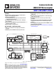
PIN FUNCTION DESCRIPTIONS
ADSP-21061 pin definitions are listed below. All pins are identi-
cal on the ADSP-21061 and ADSP-21061L. Inputs identified as
synchronous (S) must meet timing requirements with respect to
CLKIN (or with respect to TCK for TMS, TDI). Inputs identi-
fied as asynchronous (A) can be asserted asynchronously to
CLKIN (or to TCK for TRST
).
Unused inputs should be tied or pulled to VDD or GND, except
for ADDR31-0, DATA47-0, FLAG3-0, SW
, and inputs that have
internal pull-up or pull-down resistors (CPA
, ACK, DTx, DRx,
TCLKx, RCLKx, TMS, and TDI)—these pins can be left float-
ing. These pins have a logic-level hold circuit that prevents the
input from floating internally.
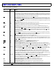
Table 2. Pin Descriptions
Pin Type Function
ADDR
31–0
I/O/T External Bus Address. The ADSP-21061 outputs addresses for external memory and peripherals on these
pins. In a multiprocessor system the bus master outputs addresses for read/write of the internal memory or
IOP registers of other ADSP-21061s. The ADSP-21061 inputs addresses when a host processor or multipro-
cessing bus master is reading or writing its internal memory or IOP registers.
DATA
47–0
I/O/T External Bus Data. The ADSP-21061 inputs and outputs data and instructions on these pins. 32-bit single-
precision floating-point data and 32-bit fixed-point data is transferred over Bits 47 to 16 of the bus. 40-bit
extended-precision floating-point data is transferred over Bits 47 to 8 of the bus. 16-bit short word data is
transferred over Bits 31 to 16 of the bus. In PROM boot mode, 8-bit data is transferred over Bits 23 to 16. Pull-
up resistors on unused DATA pins are not necessary.
MS
3–0
O/T Memory Select Lines. These lines are asserted (low) as chip selects for the corresponding banks of external
memory. Memory bank size must be defined in the ADSP-21061’s system control register (SYSCON). The
MS
3–0
lines are decoded memory address lines that change at the same time as the other address lines.
When no external memory access is occurring the MS
3–0
lines are inactive; they are active however when a
conditional memory access instruction is executed, whether or not the condition is true. MS
0
can be used
with the PAGE signal to implement a bank of DRAM memory (Bank 0). In a multiprocessing system the MS
3–0
lines are output by the bus master.
RD
I/O/T Memory Read Strobe. This pin is asserted (low) when the ADSP-21061 reads from external memory devices
or from the internal memory of other ADSP-21061s. External devices (including other ADSP-21061s) must
assert RD
to read from the ADSP-21061’s internal memory. In a multiprocessing system RD is output by the
bus master and is input by all other ADSP-21061s.
WR
I/O/T Memory Write Strobe. This pin is asserted (low) when the ADSP-21061 writes to external memory devices
or to the internal memory of other ADSP-21061s. External devices must assert WR to write to the
ADSP-21061’s internal memory. In a multiprocessing system WR
is output by the bus master and is input by
all other ADSP-21061s.
PAGE O/T DRAM Page Boundary. The ADSP-21061 asserts this pin to signal that an external DRAM page boundary
has been crossed. DRAM page size must be defined in the ADSP-21061’s memory control register (WAIT).
DRAM can only be implemented in external memory Bank 0; the PAGE signal can only be activated for
Bank 0 accesses. In a multiprocessing system PAGE is output by the bus master.
ADRCLK O/T Clock Output Reference. In a multiprocessing system ADRCLK is output by the bus master.
SW
I/O/T Synchronous Write Select. This signal is used to interface the ADSP-21061 to synchronous memory devices
(including other ADSP-21061s). The ADSP-21061 asserts SW (low) to provide an early indication of an
impending write cycle, which can be aborted if WR
is not later asserted (e.g., in a conditional write
instruction). In a multiprocessing system, SW
is output by the bus master and is input by all other
ADSP-21061s to determine if the multiprocessor memory access is a read or write. SW is asserted at the same
time as the address output. A host processor using synchronous writes must assert this pin when writing to
the ADSP-21061(s).
A = Asynchronous, G = Ground, I = Input, O = Output, P = Power Supply, S = Synchronous, (A/D) = Active Drive, (O/D) = Open-Drain,
T = Three-State (when SBTS
is asserted, or when the ADSP-21061 is a bus slave)