
Datasheet


Rev. F | Page 22 of 64 | March 2008
ADSP-21060/ADSP-21060L/ADSP-21062/ADSP-21062L/ADSP-21060C/ADSP-21060LC
Clock Input
Reset
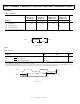
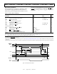
Table 9. Clock Input
Parameter
ADSP-21060
ADSP-21062
40 MHz, 5 V
ADSP-21060
ADSP-21062
33 MHz, 5 V
ADSP-21060L
ADSP-21062L
40 MHz, 3.3 V
ADSP-21060L
ADSP-21062L
33 MHz, 3.3 V
UnitMinMaxMinMaxMinMaxMinMax
Timing Requirements
t
CK
CLKIN Period 25 100 30 100 25 100 30 100 ns
t
CKL
CLKIN Width Low 7 7 8.75 8.75
1
ns
t
CKH
CLKIN Width High5555ns
t
CKRF
CLKIN Rise/Fall (0.4 V to 2.0 V) 3 3 3 3 ns
1
For the ADSP-21060LC, this specification is 9.5 ns min.
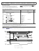
Figure 9. Clock Input
CLKIN
t
CKH
t
CKL
t
CK
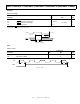
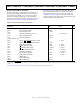
Table 10. Reset
5 V and 3.3 V
Unit
Parameter Min Max
Timing Requirements
t
WRST
RESET Pulse Width Low
1
4t
CK
ns
t
SRST
RESET Setup Before CLKIN High
2
14 + DT/2 t
CK
ns
1
Applies after the power-up sequence is complete. At power-up, the processor’s internal phase-locked loop requires no more than 100 μs while RESET is low, assuming stable
V
DD
and CLKIN (not including start-up time of external clock oscillator).
2
Only required if multiple ADSP-2106xs must come out of reset synchronous to CLKIN with program counters (PC) equal. Not required for multiple ADSP-2106xs commu-
nicating over the shared bus (through the external port), because the bus arbitration logic automatically synchronizes itself after reset.
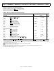
Figure 10. Reset
CLKIN
RESET
t
WRST
t
SRST