
Datasheet


ADSP-21060/ADSP-21060L/ADSP-21062/ADSP-21062L/ADSP-21060C/ADSP-21060LC
Rev. F | Page 27 of 64 | March 2008
Synchronous Read/Write—Bus Master
Use these specifications for interfacing to external memory sys-
tems that require CLKIN—relative timing or for accessing a
slave ADSP-2106x (in multiprocessor memory space). These
synchronous switching characteristics are also valid during
asynchronous memory reads and writes except where noted (see
Memory Read—Bus Master on Page 25 and Memory Write—
Bus Master on Page 26). When accessing a slave ADSP-2106x,
these switching
characteristics must meet the slave’s timing
requirements for synchronous read/writes (see Synchronous
Read/Write—Bus Slave on Page 29). The slave ADSP-2106x
must also meet these (bus master) timing requirements for data
and acknowledge setup and hold times.
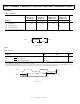
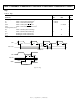
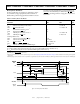
Table 16. Synchronous Read/Write—Bus Master
5 V and 3.3 V
Unit
Parameter Min Max
Timing Requirements
t
SSDATI
Data Setup Before CLKIN 3 + DT/8 ns
t
HSDATI
Data Hold After CLKIN 3.5 – DT/8 ns
t
DAAK
ACK Delay After Address, Selects
1, 2
14 + 7DT/8 + W ns
t
SACKC
ACK Setup Before CLKIN
2
6.5+DT/4 ns
t
HACK
ACK Hold After CLKIN –1 – DT/4 ns
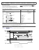
Switching Characteristics
t
DADRO
Address, MSx, BMS, SW Delay After CLKIN
1
7 – DT/8 ns
t
HADRO
Address, MSx, BMS, SW Hold After CLKIN –1 – DT/8 ns
t
DPGC
PAGE Delay After CLKIN 9 + DT/8 16 + DT/8 ns
t
DRDO
RD High Delay After CLKIN –2 – DT/8 4 – DT/8 ns
t
DWRO
WR High Delay After CLKIN –3 – 3DT/16 4 – 3DT/16 ns
t
DRWL
RD/WR Low Delay After CLKIN 8 + DT/4 12.5 + DT/4 ns
t
SDDATO
Data Delay After CLKIN 19 + 5DT/16 ns
t
DATTR
Data Disable After CLKIN
3
0 – DT/8 7 – DT/8 ns
t
DADCCK
ADRCLK Delay After CLKIN 4 + DT/8 10 + DT/8 ns
t
ADRCK
ADRCLK Period t
CK
ns
t
ADRCKH
ADRCLK Width High (t
CK
/2 – 2) ns
t
ADRCKL
ADRCLK Width Low (t
CK
/2 – 2) ns
1
The falling edge of MSx, SW, BMS is referenced.
2
ACK delay/setup: user must meet t
DAAK
or t
DSAK
or synchronous specification t
SAKC
for deassertion of ACK (low), all three specifications must be met for assertion of ACK
(high).
3
See Example System Hold Time Calculation on Page 47 for calculation of hold times given capacitive and dc loads.