a DSP Microcomputer ADSP-21065L SDRAM Controller for Glueless Interface to Low Cost External Memory (@ 66 MHz) 64M Words External Address Range 12 Programmable I/O Pins and Two Timers with Event Capture Options Code-Compatible with ADSP-2106x Family 208-Lead MQFP or 196-Ball Mini-BGA Package 3.
ADSP-21065L Host Processor Interface Efficient Interface to 8-, 16-, and 32-Bit Microprocessors Host Can Directly Read/Write ADSP-21065L IOP Registers 544 Kbits Configurable On-Chip SRAM Dual-Ported for Independent Access by Core Processor and DMA Configurable in Combinations of 16-, 32-, 48-Bit Data and Program Words in Block 0 and Block 1 Multiprocessing Distributed On-Chip Bus Arbitration for Glueless, Parallel Bus Connect Between Two ADSP-21065Ls Plus Host 132 Mbytes/s Transfer Rate Over Parallel Bus
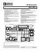
ADSP-21065L ADSP-21065L #1 CLKIN RESET RESET 01 ID1-0 SPORT0 TX0_A TX0_B RX0_A RX0_B The ADSP-21065L is fabricated in a high speed, low power CMOS process, 0.35 mm technology. With its on-chip instruction cache, the processor can execute every instruction in a single cycle. Table I lists the performance benchmarks for the ADSP-21065L.
ADSP-21065L structures required in digital signal processing, and are commonly used in digital filters and Fourier transforms. The ADSP-21065L’s two DAGs contain sufficient registers to allow the creation of up to 32 circular buffers (16 primary register sets, 16 secondary). The DAGs automatically handle address pointer wraparound, reducing overhead, increasing performance, and simplifying implementation. Circular buffers can start and end at any memory location.
ADSP-21065L I/O transfers). Programs can be downloaded to the ADSP-21065L using DMA transfers. Asynchronous off-chip peripherals can control two DMA channels using DMA Request/Grant lines (DMAR1-2, DMAG1-2). Other DMA features include interrupt generation on completion of DMA transfers and DMA chaining for automatically linked DMA transfers.
ADSP-21065L ADSP-21065L #2 CLKIN RESET 10 ADDR23-0 DATA31-0 ID1-0 CONTROL SPORT0 SPORT1 RESET ID1-0 ADDR23-0 DATA RESET ADDRESS CLKIN CONTROL ADSP-21065L #1 CLOCK 01 CPA BR2 BR1 CS ADDR DATA HOST PROCESSOR (OPTIONAL) DATA31-0 SPORT0 SPORT1 CONTROL RD WR ACK MS3-0 BMS SBTS SW CS HBR HBG REDY RAS CAS DQM SDWE SDCLK1-0 SDCKE SDA10 BOOT EPROM (OPTIONAL) CS ADDR DATA ADDR DATA CS SDRAM (OPTIONAL) RAS CAS DQM WE CLK CKE A10 CPA BR2 BR1 Figure 3. Multiprocessing System –6– REV.
ADSP-21065L PIN DESCRIPTIONS ADSP-21065L pin definitions are listed below. Inputs identified as synchronous (S) must meet timing requirements with respect to CLKIN (or with respect to TCK for TMS, TDI). Inputs identified as asynchronous (A) can be asserted asynchronously to CLKIN (or to TCK for TRST).
ADSP-21065L Pin Type Function HBR I/A Host Bus Request. Must be asserted by a host processor to request control of the ADSP21065L’s external bus. When HBR is asserted in a multiprocessing system, the ADSP-21065L that is bus master will relinquish the bus and assert HBG. To relinquish the bus, the ADSP21065L places the address, data, select, and strobe lines in a high impedance state. It does, however, continue to drive the SDRAM control pins.
ADSP-21065L Pin Type Function BMS I/O/T* Boot Memory Select. Output: used as chip select for boot EPROM devices (when BSEL = 1). In a multiprocessor system, BMS is output by the bus master. Input: When low, indicates that no booting will occur and that the ADSP-21065L will begin executing instructions from external memory. See following table. This input is a system configuration selection which should be hardwired. *Three-statable only in EPROM boot mode (when BMS is an output).
ADSP-21065L Pin Type Function SDA10 O/T SDRAM A10 Pin. Enables applications to refresh an SDRAM in parallel with a host access. XTAL O Crystal Oscillator Terminal. Used in conjunction with CLKIN to enable the ADSP-21065L’s internal clock generator or to disable it to use an external clock source. See CLKIN. PWM_EVENT1-0 I/O/A PWM Output/Event Capture. In PWMOUT mode, is an output pin and functions as a timer counter.
ADSP-21065L The BTMS, BTCK, BTRST and BTDI signals are provided so that the test access port can also be used for board-level testing. When the connector is not being used for emulation, place jumpers between the Bxxx pins and the xxx pins. If you are not going to use the test access port for board testing, tie BTRST to GND and tie or pull-up BTCK to VDD. The TRST pin must be asserted after power-up (through BTRST on the connector) or held low for proper operation of the ADSP-2106x.
ADSP-21065L–SPECIFICATIONS RECOMMENDED OPERATING CONDITIONS Test Conditions Parameter VDD TCASE Supply Voltage Case Operating Temperature VIH VIL1 VIL2 High Level Input Voltage Low Level Input Voltage1 Low Level Input Voltage2 @ VDD = max @ VDD = min @ VDD = min Min C Grade Max K Grade Min Max Unit 3.13 –40 3.60 +100 3.13 0 3.60 +85 V ∞C 2.0 –0.5 –0.5 VDD + 0.5 0.8 0.7 2.0 –0.5 –0.5 VDD + 0.5 0.8 0.7 V V V NOTE See Environmental Conditions for information on thermal specifications.
ADSP-21065L POWER DISSIPATION ADSP-21065L These specifications apply to the internal power portion of VDD only. See the Power Dissipation section of this data sheet for calculation of external supply current and total supply current. For a complete discussion of the code used to measure power dissipation, see the technical note SHARC Power Dissipation Measurements. Specifications are based on the following operating scenarios: Table II.
ADSP-21065L Switching Characteristics specify how the processor changes its signals. You have no control over this timing—circuitry external to the processor must be designed for compatibility with these signal characteristics. Switching characteristics tell you what the processor will do in a given circumstance. You can also use switching characteristics to ensure that any timing requirement of a device connected to the processor (such as memory) is satisfied.
ADSP-21065L CLKIN t SIR t HIR IRQ2-0 t IPW Figure 9. Interrupts Parameter Min Timer Timing Requirements: tSTI Timer Setup Before SDCLK High tHTI Timer Hold After SDCLK High 0.0 6.0 Switching Characteristics: Timer Delay After SDCLK High tDTEX tHTEX Timer Hold After SDCLK High –5.0 Parameter Min Flags Timing Requirements: tSFI FLAG11-0IN Setup Before SDCLK High1 tHFI FLAG11-0IN Hold After SDCLK High1 –2.0 6.
ADSP-21065L Memory Read—Bus Master Use these specifications for asynchronous interfacing to memories (and memory-mapped peripherals) without reference to CLKIN. These specifications apply when the ADSP-21065L is the bus master when accessing external memory space. These switching characteristics also apply for bus master synchronous read/write timing (see Synchronous Read/Write—Bus Master below). If these timing requirements are met, the synchronous read/write timing can be ignored (and vice versa).
ADSP-21065L Memory Write—Bus Master Use these specifications for asynchronous interfacing to memories (and memory-mapped peripherals) without reference to CLKIN. These specifications apply when the ADSP-21065L is the bus master when accessing external memory space. These switching characteristics also apply for bus master synchronous read/write timing (see Synchronous Read/Write—Bus Master below). If these timing requirements are met, the synchronous read/write timing can be ignored (and vice versa).
ADSP-21065L Synchronous Read/Write—Bus Master Use these specifications for interfacing to external memory systems that require CLKIN-relative timing or for accessing a slave ADSP-21065L (in multiprocessor memory space). These synchronous switching characteristics are also valid during asynchronous memory reads and writes (see Memory Read—Bus Master and Memory Write—Bus Master).
ADSP-21065L CLKIN t HADRO t DAAK t DADRO ADDRESS SW t HACKC t SACKC ACK (IN) READ CYCLE t DRWL t DRDO RD t HSDATI t SSDATI DATA (IN) WRITE CYCLE t DWRO t DRWL WR t DATTR t DDATO DATA (OUT) Figure 13. Synchronous Read/Write—Bus Master REV.
ADSP-21065L Synchronous Read/Write—Bus Slave Use these specifications for ADSP-21065L bus master accesses of a slave’s IOP registers or internal memory (in multiprocessor memory space). The bus master must meet these (bus slave) timing requirements.
ADSP-21065L CLKIN t SADRI t HADRI ADDRESS SW t DACK t ACKTR ACK READ ACCESS t SRWLI t HRWLI t RWHPI RD t SDDATO t DATTR DATA (OUT) WRITE ACCESS t SRWLI t HRWLI WR t SDATWH DATA (IN) Figure 14. Synchronous Read/Write—Bus Slave REV.
ADSP-21065L Multiprocessor Bus Request and Host Bus Request Use these specifications for passing of bus mastership between multiprocessing ADSP-21065Ls (BRx) or a host processor (HBR, HBG). Parameter Min Timing Requirements: tHBGRCSV HBG Low to RD/WR/CS Valid1 HBR Setup Before CLKIN2 tSHBRI tHHBRI HBR Hold Before CLKIN2 tSHBGI HBG Setup Before CLKIN HBG Hold Before CLKIN High tHHBGI tSBRI BRx, CPA Setup Before CLKIN3 tHBRI BRx, CPA Hold Before CLKIN High Max Unit 20.
ADSP-21065L CLKIN t SHBRI t HHBRI HBR t DHBGO t HHBGO HBG (OUT) t DBRO t HBRO BRx (OUT) t DCPAO t TRCPA CPA (OUT) (O/D) t SHBGI t HHBGI HBG (IN) t SBRI t HBRI BRx (IN) CPA (IN) (O/D) HBR CS t TRDYHG t DRDYCS REDY (O/D) t ARDYTR REDY (A/D) t HBGRCSV HBG (OUT) RD WR CS O/D = OPEN DRAIN, A/D = ACTIVE DRIVE Figure 15. Multiprocessor Bus Request and Host Bus Request REV.
ADSP-21065L Asynchronous Read/Write—Host to ADSP-21065L Use these specifications for asynchronous host processor accesses of an ADSP-21065L, after the host has asserted CS and HBR (low). After the ADSP-21065L returns HBG, the host can drive the RD and WR pins to access the ADSP-21065L’s IOP registers. HBR and HBG are assumed low for this timing. Writes can occur at a minimum interval of (1/2) tCK.
ADSP-21065L READ CYCLE ADDRESS/CS tHADRDH tSADRDL tWRWH RD tHDARWH DATA (OUT) tSDATRDY tDRDYRDL tDRDHRDY tRDYPRD REDY (O/D) REDY (A/D) WRITE CYCLE ADDRESS tSADWRH tSCSWRL tHADWRH tHCSWRH CS tWWRL tWRWH WR tHDATWH tSDATWH DATA (IN) tDWRHRDY tDRDYWRL tRDYPWR REDY (O/D) REDY (A/D) O/D = OPEN DRAIN, A/D = ACTIVE DRIVE Figure 16. Asynchronous Read/Write—Host to ADSP-21065L REV.
ADSP-21065L Three-State Timing—Bus Master, Bus Slave, HBR, SBTS These specifications show how the memory interface is disabled (stops driving) or enabled (resumes driving) relative to CLKIN and the SBTS pin. This timing is applicable to bus master transition cycles (BTC) and host transition cycles (HTC) as well as the SBTS pin. Parameter Min Timing Requirements: tSTSCK SBTS Setup Before CLKIN tHTSCK SBTS Hold Before CLKIN 7.
ADSP-21065L CLKIN t STSCK t HTSCK SBTS t MIENA, t MIENS, t MIENHG t MITRA, t MITRS, t MITRHG MEMORY INTERFACE t DATTR t DATEN DATA t ACKTR t ACKEN ACK HBG tMTRHBG t MENHBG MEMORY INTERFACE MEMORY INTERFACE = ADDRESS, RD, WR, MSx, SW, DMAGx. BMS (IN EPROM BOOT MODE) Figure 17. Three-State Timing REV.
ADSP-21065L DMA Handshake These specifications describe the three DMA handshake modes. In all three modes DMAR is used to initiate transfers. For handshake mode, DMAG controls the latching or enabling of data externally. For external handshake mode, the data transfer is controlled by the ADDR23-0, RD, WR, SW, MS3-0, ACK, and DMAG signals. External mode cannot be used for transfers with SDRAM. For Paced Master mode, the data transfer is controlled by ADDR23-0, RD, WR, MS3-0, and ACK (not DMAG).
ADSP-21065L CLKIN t SDRLC t DMARLL t SDRHC t WDR t DMARH DMARx t HDGC t DDGL t WDGL t WDGH DMAGx TRANSFERS BETWEEN ADSP-2106x INTERNAL MEMORY AND EXTERNAL DEVICE t VDATDGH t DATRDGH DATA (FROM ADSP-2106x TO EXTERNAL DEVICE) t DATDRH t HDATIDG t SDATDGL DATA (FROM EXTERNAL DEVICE TO ADSP-2106x) TRANSFERS BETWEEN EXTERNAL DEVICE AND EXTERNAL MEMORY *(EXTERNAL HANDSHAKE MODE) t DGWRL WR (EXTERNAL DEVICE TO EXTERNAL MEMORY) RD (EXTERNAL MEMORY TO EXTERNAL DEVICE) t DGWRH t DGWRR t DGRDR t DGRD
ADSP-21065L SDRAM Interface—Bus Master Use these specifications for ADSP-21065L bus master accesses of SDRAM. Parameter Min Timing Requirements: tSDSDK Data Setup Before SDCLK tHDSDK Data Hold After SDCLK 2.0 1.
ADSP-21065L CLKIN t DSDK2 t DSDK1 t SDKH t SDK SDCLK t SDSDK t SDKL t HDSDK DATA (IN) t SDTRSDK t DCADSDK t SDENSDK t HCADSDK DATA (OUT) t DCADSDK CMND1 ADDR (OUT) t HCADSDK t SDCEN t SDCTR CMND1 (OUT) ADDR (OUT) t SDAEN t SDATR CLKIN t SSDKC2 t SSDKC1 SDCLK (IN) t SCSDK CMND2 (IN) t HCSDK NOTES 1COMMAND = SDCKE, MS , RAS, CAS, SDWE, DQM, AND SDA10. X 2SDRAM CONTROLLER ADDS ONE SDRAM CLK THREE-STATED CYCLE DELAY (t /2) ON A READ FOLLOWED BY A WRITE. CK Figure 19.
ADSP-21065L Serial Ports Parameter Min External Clock Timing Requirements: TFS/RFS Setup Before TCLK/RCLK1 tSFSE tHFSE TFS/RFS Hold After TCLK/RCLK1 tSDRE Receive Data Setup Before RCLK1 Receive Data Hold After RCLK1 tHDRE tSCLKW TCLK/RCLK Width tSCLK TCLK/RCLK Period 4.0 4.0 1.5 4.0 9.
ADSP-21065L DATA RECEIVE– INTERNAL CLOCK DATA RECEIVE– EXTERNAL CLOCK SAMPLE EDGE DRIVE EDGE DRIVE EDGE SAMPLE EDGE tSCLKIW tSCLKW RCLK RCLK tDFSE tHOFSE tSFSI tDFSE tHOFSE tHFSI RFS tSFSE tHFSE tSDRE tHDRE RFS tSDRI tHDRI DR DR NOTE: EITHER THE RISING EDGE OR FALLING EDGE OF RCLK, TCLK CAN BE USED AS THE ACTIVE SAMPLING EDGE.
ADSP-21065L EXTERNAL RFS with MCE = 1, MFD = 0 DRIVE DRIVE SAMPLE RCLK tHOFSE/I tSFSE/I RFS tDDTE/I tHDTE/I tDTENLFSE 1ST BIT DT 2ND BIT tDDTLFSE LATE EXTERNAL TFS DRIVE DRIVE SAMPLE TCLK tHOFSE/I tSFSE/I TFS tDDTE/I tHDTE/I tDTENLFSE 1ST BIT DT 2ND BIT tDDTLFSE Figure 21.
ADSP-21065L JTAG Test Access Port and Emulation Parameter Min Timing Requirements: tTCK TCK Period TDI, TMS Setup Before TCK High tSTAP tHTAP TDI, TMS Hold After TCK High tSSYS System Inputs Setup Before TCK Low1 System Inputs Hold After TCK Low1 tHSYS tTRSTW TRST Pulsewidth tCK 3.0 3.0 7.0 12.0 4 tCK Max Unit ns ns ns ns ns ns Switching Characteristics: TDO Delay from TCK Low tDTDO tDSYS System Outputs Delay After TCK Low2 11.0 15.
ADSP-21065L OUTPUT DRIVE CURRENT Example System Hold Time Calculation To determine the data output hold time in a particular system, first calculate tDECAY using the equation given above. Choose DV to be the difference between the ADSP-21065L’s output voltage and the input threshold for the device requiring the hold time. A typical DV will be 0.4 V. CL is the total bus capacitance (per data line), and IL is the total leakage or three-state current (per data line).
ADSP-21065L Capacitive Loading 8.0 7.0 RISE AND FALL TIMES – ns Output delays and holds are based on standard capacitive loads: 50 pF on all pins. The delay and hold specifications given should be derated by a factor of l.8 ns/50 pF for loads other than the nominal value of 50 pF. Figure 28 and Figure 29 show how output rise time varies with capacitance. Figure 30 shows graphically how output delays and hold vary with load capacitance.
ADSP-21065L A typical power consumption can now be calculated for these conditions by adding a typical internal power dissipation. (IDDIN see calculation in Electrical Characteristics section): POWER DISSIPATION Total power dissipation has two components: one due to internal circuitry and one due to the switching of external output drivers. Internal power dissipation depends on the sequence in which instructions execute and the data operands involved.
ADSP-21065L 208-LEAD MQFP PIN CONFIGURATION Pin No. Pin Name Pin No. Pin Name Pin No. Pin Name Pin No. Pin Name Pin No.
ADSP-21065L 159 GND 158 VDD 157 RESET 160 ADDR23 161 ADDR22 162 ADDR21 163 VDD 165 ADDR19 164 ADDR20 167 GND 166 ADDR18 168 GND 169 ADDR17 171 ADDR15 170 ADDR16 173 ADDR14 172 VDD 175 ADDR12 174 ADDR13 176 VDD 177 GND 178 ADDR11 181 GND 180 ADDR9 179 ADDR10 183 ADDR8 182 VDD 185 ADDR6 184 ADDR7 187 GND 186 GND 189 ADDR4 188 ADDR5 191 VDD 190 ADDR3 193 ADDR2 192 VDD 195 ADDR0 194 ADDR1 197 FLAG0 196 GND 200 VDD 199 FLAG2 198 FLAG1 202 NC 201 FLAG3 204 GND 203 NC 1 156 2 155
ADSP-21065L OUTLINE DIMENSIONS 208-Lead Metric Quad Flat Package [MQFP] (S-208-2) Dimensions shown in millimeters 0.75 0.60 0.45 30.85 30.60 SQ 30.35 4.10 MAX 208 157 156 1 SEATING PLANE PIN 1 INDICATOR 28.20 28.00 SQ 27.80 TOP VIEW (PINS DOWN) VIEW A 3.60 3.40 3.20 0.50 0.25 53 0.50 BSC (LEAD PITCH) 0.08 MAX (LEAD COPLANARITY) 0.27 0.17 (LEAD WIDTH) VIEW A ROTATED 90ⴗ CCW REV. C 105 104 52 0.20 0.09 NOTES: 1. THE ACTUAL POSITION OF EACH LEAD IS WITHIN 0.
ADSP-21065L 196-BALL MINI-BGA PIN CONFIGURATION Ball # Name Ball # Name Ball # Name Ball # Name Ball # Name A1 A2 A3 A4 A5 A6 A7 A8 A9 A10 A11 A12 A13 A14 NC1 NC2 FLAG2 ADDR0 ADDR3 ADDR6 ADDR7 ADDR8 ADDR11 ADDR14 ADDR17 ADDR18 NC8 NC7 B1 B2 B3 B4 B5 B6 B7 B8 B9 B10 B11 B12 B13 B14 DR0A RFS0 IRQ0 FLAG0 ADDR2 ADDR5 ADDR9 ADDR12 ADDR15 ADDR19 ADDR21 ADDR23 GND TCK C1 C2 C3 C4 C5 C6 C7 C8 C9 C10 C11 C12 C13 C14 TCLK0 RCLK0 IRQ2 FLAG3 ADDR1 ADDR4 ADDR10 ADDR13 ADDR16 ADDR20 ADDR22 RESET BSEL TDO
ADSP-21065L 196-BALL MINI-BGA PIN CONFIGURATION REV.
ADSP-21065L Part Number Case Temperature Range Instruction Rate On-Chip SRAM Operating Voltage Package Options ADSP-21065LKS-240 ADSP-21065LCS-240 ADSP-21065LKCA-240 ADSP-21065LKS-264 ADSP-21065LKCA-264 ADSP-21065LCCA-240 0°C to +85°C –40°C to +100°C 0°C to +85°C 0°C to +85°C 0°C to +85°C –40°C to +100°C 60 MHz 60 MHz 60 MHz 66 MHz 66 MHz 60 MHz 544 Kbit 544 Kbit 544 Kbit 544 Kbit 544 Kbit 544 Kbit 3.3 V 3.3 V 3.3 V 3.3 V 3.3 V 3.