
Datasheet


–41–REV. 0
ADSP-21160N
where:
• P
EXT
is from Table 30
• P
INT
is I
DDINT
× 1.9 V, using the calculation I
DDINT
listed in
Power Dissipation on Page 40
• P
PLL
is AI
DD
× 1.9 V, using the value for AI
DD
listed in
ABSOLUTE MAXIMUM RATINGS on Page 15
Note that the conditions causing a worst-case
P
EXT
are different
from those causing a worst-case P
INT
. Maximum P
INT
cannot
occur while 100% of the output pins are switching from all ones
to all zeros. Note also that it is not common for an application to
have 100% or even 50% of the outputs switching simultaneously.
Test Conditions
The test conditions for timing parameters appearing in ADSP-
21160N specifications on Page 14 include output disable time,
output enable time, and capacitive loading.
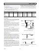
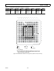
Output Disable Time
Output pins are considered to be disabled when they stop driving,
go into a high impedance state, and start to decay from their
output high or low voltage. The time for the voltage on the bus
to decay by
∆
V
is dependent on the capacitive load,
C
L
and the
load current,
I
L
. This decay time can be approximated by the
following equation:
t
DECAY
= (C
L
∆V)/I
L
The output disable time t
DIS
is the difference between t
MEASURED
and
t
DECAY
as shown in Figure 28. The time t
MEASURED
is the
interval from when the reference signal switches to when the
output voltage decays
∆
V
from the measured output high or
output low voltage.
t
DECAY
is calculated with test loads
C
L
and
I
L
,
and with
∆
V
equal to 0.5 V.
Output Enable Time
Output pins are considered to be enabled when they have made
a transition from a high impedance state to when they start
driving. The output enable time t
ENA
is the interval from when a
reference signal reaches a high or low voltage level to when the
output has reached a specified high or low trip point, as shown
in the Output Enable/Disable diagram (Figure 28). If multiple
pins (such as the data bus) are enabled, the measurement value
is that of the first pin to start driving.
Example System Hold Time Calculation
To determine the data output hold time in a particular system,
first calculate t
DECAY
using the equation given above. Choose
∆
V
to be the difference between the ADSP-21160N’s output voltage
and the input threshold for the device requiring the hold time. A
typical
∆
V will be 0.4 V.
C
L
is the total bus capacitance (per data
line), and
I
L
is the total leakage or three-state current (per data
line). The hold time will be
t
DECAY
plus the minimum disable time
(i.e., t
DATRWH
for the write cycle).
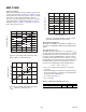
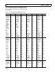
Table 30. External Power Calculations (3.3 V Device)
Pin Type No. of Pins % Switching × C × f × V
DD
2
= P
EXT
Address 15 50 × 44.7 pF × 24 MHz × 10.9 V = 0.088 W
MS0 1 0 × 44.7 pF × 24 MHz × 10.9 V = 0.000 W
WRx
2 × 44.7 pF × 24 MHz × 10.9 V = 0.023 W
Data 64 50 × 14.7 pF × 24 MHz × 10.9 V = 0.123 W
CLKOUT 1 × 4.7 pF × 48 MHz × 10.9 V = 0.003 W
P
EXT
= 0.237 W
Figure 28. Output Enable/Disable
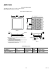
Figure 29. Equivalent Device Loading for AC
Measurements (Includes All Fixtures)
Figure 30. Voltage Reference Levels for AC Measurements
(Except Output Enable/Disable)
REFERENCE
SIGNAL
t
DIS
OUTPUT STARTS
DRIVING
V
OH
(MEASURED) – V
V
OL
(MEASURED) + V
t
MEASURED
V
OH
(MEASURED)
V
OL
(MEASURED)
2.0V
1.0V
HIGH IMPEDANCE STATE.
TEST CONDITIONS CAUSE THIS VOLTAGE
TO BE APPROXIMATELY 1.5V
OUTPUT STOPS
DRIVING
t
DECAY
t
ENA
1.5V
30pF
TO
OUTPUT
PIN
50
INPUT
OR
OUTPUT
1.5V 1.5V