
Datasheet


ADSP-21161N
Rev. C | Page 3 of 60 | January 2013
GENERAL DESCRIPTION
The ADSP-21161N SHARC
®
DSP is a low cost derivative of the
ADSP-21160 featuring Analog Devices Super Harvard Archi-
tecture. Easing portability, the ADSP-21161N is source code
compatible with the ADSP-21160 and with first generation
ADSP-2106x SHARC processors in SISD (Single-Instruction,
Single-Data) mode. Like other SHARC DSPs, the ADSP-
21161N is a 32-bit processor that is optimized for high perfor-
mance DSP applications. The ADSP-21161N includes a
100 MHz or 110 MHz core, a dual-ported on-chip SRAM, an
integrated I/O processor with multiprocessing support, and
multiple internal buses to eliminate I/O bottlenecks.
As was first offered in the ADSP-21160, the ADSP-21161N
offers a single-instruction multiple-data (SIMD) architecture.
Using two computational units (ADSP-2106x SHARC proces-
sors have one), the ADSP-21161N can double cycle
performance versus the ADSP-2106x on a range of DSP
algorithms.
Fabricated in a state of the art, high speed, low power CMOS
process, the ADSP-21161N has a 10 ns or 9 ns instruction cycle
time. With its SIMD computational hardware running at
110 MHz, the ADSP-21161N can perform 660 million floating-
point operations per second. Table 1 shows performance bench-
marks for the ADSP-21161N.
These benchmarks provide single-channel extrapolations of
measured dual-channel processing performance. For more
information on benchmarking and optimizing DSP code, for
both single and dual-channel processing, see the Analog Devices
Inc. website.
The ADSP-21161N continues SHARC’s industry-leading stan-
dards of integration for DSPs, combining a high performance
32-bit DSP core with integrated, on-chip system features. These
features include a 1M bit dual ported SRAM memory, host pro-
cessor interface, I/O processor that supports 14 DMA channels,
four serial ports, two link ports, SDRAM controller, SPI inter-
face, external parallel bus, and glueless multiprocessing.
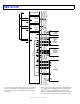
The block diagram of the ADSP-21161N on Page 1 illustrates
the following architectural features:
• Two processing elements, each made up of an ALU, multi-
plier, shifter, and data register file
• Data address generators (DAG1, DAG2)
• Program sequencer with instruction cache
• PM and DM buses capable of supporting four 32-bit data
transfers between memory and the core every core proces-
sor cycle
•Interval timer
•On-Chip SRAM (1M bit)
• SDRAM controller for glueless interface to SDRAMs
• External port that supports:
• Interfacing to off-chip memory peripherals
• Glueless multiprocessing support for six
ADSP-21161N SHARCs
• Host port read/write of IOP registers
• DMA controller
• Four serial ports
•Two link ports
• SPI compatible interface
• JTAG test access port
• 12 general-purpose I/O pins
Figure 2 shows a typical single-processor system. A multipro-
cessing system appears in Figure 5 on Page 8.
ADSP-21161N FAMILY CORE ARCHITECTURE
The ADSP-21161N includes the following architectural features
of the ADSP-2116x family core. The ADSP-21161N is code
compatible at the assembly level with the ADSP-21160,
ADSP-21060, ADSP-21061, ADSP-21062, and ADSP-21065L.
SIMD Computational Engine
The ADSP-21161N contains two computational processing ele-
ments that operate as a single-instruction multiple-data (SIMD)
engine. The processing elements are referred to as PEX and
PEY, and each contains an ALU, multiplier, shifter, and register
file. PEX is always active, and PEY may be enabled by setting the
PEYEN mode bit in the MODE1 register. When this mode is
enabled, the same instruction is executed in both processing ele-
ments, but each processing element operates on different data.
This architecture is efficient at executing math intensive DSP
algorithms.
Entering SIMD mode also has an effect on the way data is trans-
ferred between memory and the processing elements. When in
SIMD mode, twice the data bandwidth is required to sustain
computational operation in the processing elements. Because of
this requirement, entering SIMD mode also doubles the
bandwidth between memory and the processing elements.
Table 1. Benchmarks
Benchmark Algorithm
100 MHz
Instruction
Rate
110 MHz
Instruction
Rate
1024 Point Complex FFT
(Radix 4, with Reversal)
92 μs 83.6 μs
FIR Filter (Per Tap) 5 ns 4.5 ns
IIR Filter (Per Biquad) 20 ns 18.18 ns
Matrix Multiply (Pipelined)
[3 3] [3 1] 45 ns 40.9 ns
[4 4] [4 1] 80 ns 72.72 ns
Divide (y/x) 60 ns 54.54 ns
Inverse Square Root 40 ns 36.36 ns
DMA Transfers 800M bytes/s 880M bytes/s