
Datasheet


Rev. C | Page 6 of 60 | January 2013
ADSP-21161N
JTAG emulators provides emulation at full processor speed,
allowing inspection and modification of memory, registers, and
processor stacks. The processor’s JTAG interface ensures that
the emulator will not affect target system loading or timing.
For complete information on SHARC Analog Devices DSP
Tools product line of JTAG emulator operation, see the appro-
priate Emulator Hardware User’s Guide. For detailed infor-
mation on the interfacing of Analog Devices JTAG emulators
with Analog Devices DSP products with JTAG emulation ports,
please refer to Engineer to Engineer Note EE-68: Analog Devices
JTAG Emulation Technical Reference. Both of these documents
can be found on the Analog Devices website.
DMA Controller
The ADSP-21161N’s on-chip DMA controller enables zero-
overhead data transfers without processor intervention. The
DMA controller operates independently and invisibly to the
processor core, allowing DMA operations to occur while the
core is simultaneously executing its program instructions. DMA
transfers can occur between the ADSP-21161N’s internal mem-
ory and external memory, external peripherals, or a host
processor. DMA transfers can also occur between the ADSP-
21161N’s internal memory and its serial ports, link ports, or the
SPI-compatible (Serial Peripheral Interface) port. External bus
packing and unpacking of 32-, 48-, or 64-bit words in internal
memory is performed during DMA transfers from either 8-,
16-, or 32-bit wide external memory. Fourteen channels of
DMA are available on the ADSP-21161N—two are shared
between the SPI interface and the link ports, eight via the serial
ports, and four via the processor’s external port (for host pro-
cessor, other ADSP-21161Ns, memory, or I/O transfers).
Programs can be downloaded to the ADSP-21161N using DMA
transfers. Asynchronous off-chip peripherals can control two
DMA channels using DMA Request/Grant lines (DMAR2–1
,
DMAG2–1
). Other DMA features include interrupt generation
upon completion of DMA transfers, and DMA chaining for
automatic linked DMA transfers.
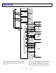
Figure 3. Memory Map
0x000A 0000
-
0x000A7FFF(BLK1)
0x0002 8000
-
0x0002 9FFF (BLK 1)
0x0005 0000
-
0x0005 3FFF (BLK 1)
0x0010 0000
-
0x0011 FFFF
0x0004 0000
-
0x0004 3FFF (BLK 0)
0x0008 0000
-
0X0008 7FFF (BLK 0)
0x0012 0000
-
0x0013 FFFF
0x0014 0000
-
0x0015 FFFF
0x0016 0000
-
0x0017 FFFF
0x001A 0000
-
0x001B FFFF
0x0000 0000
-
0x0001 FFFF
0x0002 0000
-
0x0002 1FFF (BLK 0)
0x0020 0000
BANK 1
MS0
BANK 2
MS1
BANK 3
MS2
MS3
IOP REGISTERS
LONG WORD ADDRESSING
SHORT WORD ADDRESSING
NORMAL WORD ADDRESSING
ADDRESS
BANK 0
0x03FF FFFF (SDRAM)
0x00FF FFFF (NON-SDRAM)
0x0400 0000
0x07FF FFFF (SDRAM)
0x04FF FFFF (NON-SDRAM)
0x0800 0000
0x0BFF FFFF (SDRAM)
0x08FF FFFF (NON-SDRAM)
0x0C00 0000
0x0FFF FFFF (SDRAM)
0x0CFF FFFF (NON-SDRAM)
NOTE: BANK SIZES ARE FIXED
0x0018 0000
-
0x0019 FFFF
INTERNAL
MEMORY
SPACE
MULTIPROCESSOR
MEMORY
SPACE
ADDRESS
IOP REGISTERS OF ADSP-21161N
WITH ID = 001
IOP REGISTERS OF ADSP-21161N
WITH ID = 010
IOP REGISTERS OF ADSP-21161N
WITH ID = 011
IOP REGISTERS OF ADSP-21161N
WITH ID = 100
IOP REGISTERS OF ADSP-21161N
WITH ID = 101
IOP REGISTERS OF ADSP-21161N
WITH ID = 110
RESERVED
0x001C 0000
0x001F FFFF
EXTERNAL MEMORY SPACE