
Datasheet


ADSP-21261/ADSP-21262/ADSP-21266
Rev. G | Page 4 of 48 | December 2012
elements, but each processing element operates on different
data. This architecture is efficient at executing math intensive
audio algorithms.
Entering SIMD mode also has an effect on the way data is trans-
ferred between memory and the processing elements. When in
SIMD mode, twice the data bandwidth is required to sustain
computational operation in the processing elements. Because of
this requirement, entering SIMD mode also doubles the band-
width between memory and the processing elements. When
using the DAGs to transfer data in SIMD mode, two data values
are transferred with each access of memory or the register file.
Independent, Parallel Computation Units
Within each processing element is a set of computational units.
The computational units consist of an arithmetic/logic unit
(ALU), multiplier, and shifter. These units perform all opera-
tions in a single cycle. The three units within each processing
element are arranged in parallel, maximizing computational
throughput. Single multifunction instructions execute parallel
ALU and multiplier operations. In SIMD mode, the parallel
ALU and multiplier operations occur in both processing
elements. These computation units support IEEE 32-bit single
precision floating-point, 40-bit extended precision floating-
point, and 32-bit fixed-point data formats.
Data Register File
A general-purpose data register file is contained in each
processing element. The register files transfer data between the
computation units and the data buses, and store intermediate
results. These 10-port, 32-register (16 primary, 16 secondary)
register files, combined with the ADSP-2126x enhanced Har-
vard architecture, allow unconstrained data flow between
computation units and internal memory. The registers in PEX
are referred to as R0–R15 and in PEY as S0–S15.
Single-Cycle Fetch of Instruction and Four Operands
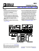
The ADSP-2126x features an enhanced Harvard architecture in
which the data memory (DM) bus transfers data and the pro-
gram memory (PM) bus transfers both instructions and data
(see Figure 1 on Page 1). With the ADSP-2126x’s separate pro-
gram and data memory buses and on-chip instruction cache,
the processor can simultaneously fetch four operands (two over
each data bus) and one instruction (from the cache), all in a
single cycle.
Instruction Cache
The ADSP-2126x includes an on-chip instruction cache that
enables three-bus operation to fetch an instruction and four
data values. The cache is selective—only the instructions whose
fetches conflict with PM bus data accesses are cached. This
cache allows full-speed execution of core, looped operations
such as digital filter multiply-accumulates, and FFT butterfly
processing.
Data Address Generators with Zero-Overhead Hardware
Circular Buffer Support
The ADSP-2126x’s two data address generators (DAGs) are
used for indirect addressing and implementing circular data
buffers in hardware. Circular buffers allow efficient program-
ming of delay lines and other data structures required in digital
signal processing, and are commonly used in digital filters and
Fourier transforms. The two DAGs of the ADSP-2126x contain
sufficient registers to allow the creation of up to 32 circular buf-
fers (16 primary register sets, 16 secondary). The DAGs
automatically handle address pointer wraparound, reduce over-
head, increase performance, and simplify implementation.
Circular buffers can start and end at any memory location.
Flexible Instruction Set
The 48-bit instruction word accommodates a variety of parallel
operations for concise programming. For example, the
ADSP-2126x can conditionally execute a multiply, an add, and a
subtract in both processing elements while branching and fetch-
ing up to four 32-bit values from memory—all in a single
instruction.
MEMORY AND I/O INTERFACE FEATURES
The ADSP-2126x adds the following architectural features to
the SIMD SHARC family core:
Dual-Ported On-Chip Memory
The ADSP-21262 and ADSP-21266 contain two megabits of
internal SRAM and four megabits of internal mask-program-
mable ROM. The ADSP-21261 contain one megabit of internal
SRAM and three megabits of internal mask-programmable
ROM. Each block can be configured for different combinations
of code and data storage (see memory maps, Table 4 and
Table 5). Each memory block is dual-ported for single-cycle,
independent accesses by the core processor and I/O processor.
The dual-ported memory, in combination with three separate
on-chip buses, allows two data transfers from the core and one
from the I/O processor, in a single cycle.
The ADSP-2126x is available with a variety of multichannel
surround sound decoders, preprogrammed in ROM memory.
Table 3 shows the configuration of decoder algorithms.
Table 3. Multichannel Surround Sound Decoder Algorithms
in On-Chip ROM
Algorithms B ROM C ROM D ROM
PCM Yes Yes Yes
AC-3 Yes Yes Yes
DTS 96/24 v2.2 v2.3 v2.3
AAC (LC) Yes Yes Coefficients only
WMAPRO 7.1 96 KHz No No Yes
MPEG2 BC 2ch Yes Yes No
Noise Yes Yes Yes
DPL2x/EX DPL2 Yes Yes
Neo:6/ES (v2.5046) Yes Yes Yes