
Datasheet


Rev. G | Page 10 of 48 | December 2012
ADSP-21261/ADSP-21262/ADSP-21266
PIN FUNCTION DESCRIPTIONS
The ADSP-2126x pin definitions are listed below. Inputs identi-
fied as synchronous (S) must meet timing requirements with
respect to CLKIN (or with respect to TCK for TMS, TDI).
Inputs identified as asynchronous (A) can be asserted asynchro-
nously to CLKIN (or to TCK for TRST
). Tie or pull unused
inputs to V
DDEXT
or GND, except for the following:
DAI_Px, SPICLK, MISO, MOSI, EMU
, TMS,TRST, TDI and
AD15–0 (NOTE: These pins have internal pull-up resistors.)
The following symbols appear in the Type column of Table 6:
A = asynchronous, G = ground, I = input, O = output,
P = power supply, S = synchronous, (A/D) = active drive,
(O/D) = open-drain, and T = three-state.
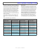
Table 6. Pin Descriptions
Pin Type
State During and
After Reset Function
AD15–0 I/O/T Rev. 0.1 silicon—
AD15–0 pins are
driven low both
during and after
reset.
Rev. 0.2 silicon—
AD15–0 pins are
three-stated and
pulled high both
during and after
reset.
Parallel Port Address/Data. The parallel port and its corresponding DMA unit output
addresses and data for peripherals on these multiplexed pins. The multiplex state is deter-
mined by the ALE pin. The parallel port can operate in either 8-bit or 16-bit mode. Each
AD pin has a 22.5 k internal pull-up resistor. See Address Data Modes on Page 13 for
details of the AD pin operation.
For 8-bit mode: ALE is automatically asserted whenever a change occurs in the upper 16
external address bits, A23–8; ALE is used in conjunction with an external latch to retain
the values of the A23–8.
For 16-bit mode: ALE is automatically asserted whenever a change occurs in the address
bits, A15–0; ALE is used in conjunction with an external latch to retain the values of the
A15–0. To use these pins as flags (FLAG15–0), set (= 1) Bit 20 of the SYSCTL register and
disable the parallel port. See Table 7 on Page 13 for a list of how the AD15–0 pins map to
the flag pins. When configured in the IDP_PDAP_CTL register, the IDP Channel 0 can use
these pins for parallel input data.
RD
O Output only, driven
high
1
Parallel Port Read Enable. RD is asserted low whenever the DSP reads 8-bit or
16-bit data from an external memory device. When AD15–0 are flags, this pin remains
deasserted.
WR O Output only, driven
high
1
Parallel Port Write Enable. WR is asserted low whenever the DSP writes 8-bit or 16-bit
data to an external memory device. When AD15–0 are flags, this pin remains deasserted.
ALE O Output only, driven
low
1
Parallel Port Address Latch Enable. ALE is asserted whenever the DSP drives a new
address on the parallel port address pin. On reset, ALE is active high. However, it can be
reconfigured using software to be active low. When AD15–0 are flags, this pin remains
deasserted.
FLAG3–0 I/O/A Three-state Flag Pins. Each FLAG pin is configured via control bits as either an input or output. As an
input, it can be tested as a condition. As an output, it can be used to signal external
peripherals. These pins can be used as an SPI interface slave select output during SPI
mastering. These pins are also multiplexed with the IRQx
and the TIMEXP signals.
In SPI master boot mode, FLAG0 is the slave select pin that must be connected to an SPI
EPROM. FLAG0 is configured as a slave select during SPI master boot. When Bit 16 is set
(= 1) in the SYSCTL register, FLAG0 is configured as IRQ0.
When Bit 17 is set (= 1) in the SYSCTL register, FLAG1 is configured as IRQ1
.
When Bit 18 is set (= 1) in the SYSCTL register, FLAG2 is configured as IRQ2
.
When Bit 19 is set (= 1) in the SYSCTL register, FLAG3 is configured as TIMEXP, which
indicates that the system timer has expired.
DAI_P20–1 I/O/T Three-state with
programmable
pull-up
Digital Application Interface Pins. These pins provide the physical interface to the SRU.
The SRU configuration registers define the combination of on-chip peripheral inputs or
outputs connected to the pin and to the pin’s output enable. The configuration registers
of these peripherals then determine the exact behavior of the pin. Any input or output
signal present in the SRU can be routed to any of these pins. The SRU provides the
connection from the serial ports, input data port, precision clock generators, and timers
to the DAI_P20–1 pins. These pins have internal 22.5 k pull-up resistors which are
enabled on reset. These pull-ups can be disabled in the DAI_PIN_PULLUP register.