
Datasheet


ADSP-21261/ADSP-21262/ADSP-21266
Rev. G | Page 3 of 48 | December 2012
GENERAL DESCRIPTION
The ADSP-21261/ADSP-21262/ADSP-21266 SHARC
®
DSPs
are members of the SIMD SHARC family of DSPs featuring
Analog Devices, Inc., Super Harvard Architecture. The
ADSP-2126x is source code compatible with the ADSP-21160
and ADSP-21161 DSPs as well as with first generation ADSP-
2106x SHARC processors in SISD (single-instruction, single-
data) mode. Like other SHARC DSPs, the ADSP-2126x are
32-bit/40-bit floating-point processors optimized for high per-
formance audio applications with dual-ported on-chip SRAM,
mask-programmable ROM, multiple internal buses to eliminate
I/O bottlenecks, and an innovative digital application interface.
Table 1 shows performance benchmarks for the processors run-
ning at 200 MHz. Table 2 shows the features of the individual
product offerings.
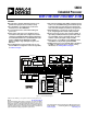
As shown in the functional block diagram in Figure 1 on Page 1,
the ADSP-2126x uses two computational units to deliver a 5 to
10 times performance increase over previous SHARC proces-
sors on a range of DSP algorithms. Fabricated in a state-of-the-
art, high speed, CMOS process, the ADSP-2126x DSPs achieve
an instruction cycle time of 5 ns at 200 MHz or 6.6 ns at
150 MHz. With its SIMD computational hardware, the
ADSP-2126x can perform 1200 MFLOPS running at 200 MHz,
or 900 MFLOPS running at 150 MHz.
The ADSP-2126x continues the SHARC family’s industry-lead-
ing standards of integration for DSPs, combining a high
performance 32-bit DSP core with integrated, on-chip system
features. These features include 2M bit dual-ported SRAM
memory, 4M bit dual-ported ROM, an I/O processor that sup-
ports 22 DMA channels, six serial ports, an SPI interface,
external parallel bus, and digital application interface.
The block diagram of the ADSP-2126x on Page 1 illustrates the
following architectural features:
• Two processing elements, each containing an ALU, multi-
plier, shifter, and data register file
• Data address generators (DAG1, DAG2)
• Program sequencer with instruction cache
• PM and DM buses capable of supporting four 32-bit data
transfers between memory and the core at every core pro-
cessor cycle
• Three programmable interval timers with PWM genera-
tion, PWM capture/pulse width measurement, and
external event counter capabilities
• On-chip dual-ported SRAM (up to 2M bit)
• On-chip dual-ported, mask-programmable ROM
(up to 4M bit)
• JTAG test access port
• 8- or 16-bit parallel port that supports interfaces to off-chip
memory peripherals
• DMA controller
• Six full-duplex serial ports (four on the ADSP-21261)
• SPI-compatible interface
• Digital application interface that includes two precision
clock generators (PCG), an input data port (IDP), six serial
ports, eight serial interfaces, a 20-bit synchronous parallel
input port, 10 interrupts, six flag outputs, six flag inputs,
three programmable timers, and a flexible signal routing
unit (SRU)
FAMILY CORE ARCHITECTURE
The ADSP-2126x is code compatible at the assembly level with
the ADSP-2136x and ADSP-2116x, and with the first generation
ADSP-2106x SHARC DSPs. The ADSP-2126x shares architec-
tural features with the ADSP-2136x and ADSP-2116x SIMD
SHARC family of DSPs, as detailed in the following sections.
SIMD Computational Engine
The ADSP-2126x contain two computational processing ele-
ments that operate as a single-instruction multiple-data (SIMD)
engine. The processing elements are referred to as PEX and PEY
and each contains an ALU, multiplier, shifter, and register file.
PEX is always active, and PEY can be enabled by setting the
PEYEN mode bit in the MODE1 register. When this mode is
enabled, the same instruction is executed in both processing
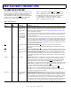
Table 1. Processor Benchmarks (at 200 MHz)
Benchmark Algorithm
Speed
(at 200 MHz)
1024 Point Complex FFT (Radix 4, with reversal) 61.3 s
FIR Filter (per tap)
1
1
Assumes two files in multichannel SIMD mode.
3.3 ns
IIR Filter (per biquad)
1
13.3 ns
Matrix Multiply (pipelined)
[3×3] × [3×1]
[4×4] × [4×1]
30 ns
53.3 ns
Divide (y/x) 20 ns
Inverse Square Root 30 ns
Table 2. ADSP-2126x SHARC Processor Features
Feature ADSP-21261 ADSP-21262 ADSP-21266
RAM 1M bit 2M bit 2M bit
ROM 3M bit 4M bit 4M bit
Audio Decoders
in ROM
1
1
For information on available audio decoding algorithms, see Table 3 on Page 4.
No No Yes
DMA Channels 18 22 22
SPORTs 4 6 6
Package 136-ball BGA
144-lead LQFP
136-ball BGA
144-lead LQFP
136-ball BGA
144-lead LQFP