
Datasheet


ADSP-21261/ADSP-21262/ADSP-21266
Rev. G | Page 7 of 48 | December 2012
Serial Peripheral (Compatible) Interface
The serial peripheral interface is an industry-standard synchro-
nous serial link, enabling the ADSP-2126x SPI-compatible port
to communicate with other SPI-compatible devices. SPI is an
interface consisting of two data pins, one device select pin, and
one clock pin. It is a full-duplex synchronous serial interface,
supporting both master and slave modes. The SPI port can
operate in a multimaster environment by interfacing with up to
four other SPI-compatible devices, either acting as a master or
slave device. The ADSP-2126x SPI-compatible peripheral
implementation also features programmable baud rates at up to
50 MHz for a core clock of 200 MHz and up to 37.5 MHz for a
core clock of 150 MHz, clock phases, and polarities. The
ADSP-2126x SPI-compatible port uses open-drain drivers to
support a multimaster configuration and to avoid data
contention.
Parallel Port
The parallel port provides interfaces to SRAM and peripheral
devices. The multiplexed address and data pins (AD15–0) can
access 8-bit devices with up to 24 bits of address, or 16-bit
devices with up to 16 bits of address. In either mode, 8- or 16-
bit, the maximum data transfer rate is one-third the core clock
speed. As an example, a clock rate of 200 MHz is equivalent to
66M byte/sec, and a clock rate of 150 MHz is equivalent to
50M byte/sec.
DMA transfers are used to move data to and from internal
memory. Access to the core is also facilitated through the paral-
lel port register read/write functions. The RD
, WR, and ALE
(address latch enable) pins are the control pins for the
parallel port.
Timers
The ADSP-2126x has a total of four timers: a core timer able to
generate periodic software interrupts, and three general-pur-
pose timers that can generate periodic interrupts and be
independently set to operate in one of three modes:
• Pulse waveform generation mode
• Pulse width count/capture mode
• External event watchdog mode
The core timer can be configured to use FLAG3 as a timer
expired output signal, and each general-purpose timer has one
bidirectional pin and four registers that implement its mode of
operation: a 6-bit configuration register, a 32-bit count register,
a 32-bit period register, and a 32-bit pulse width register. A sin-
gle control and status register enables or disables all three
general-purpose timers independently.
ROM-Based Security
The ADSP-2126x has a ROM security feature that provides
hardware support for securing user software code by preventing
unauthorized reading from the internal code when enabled.
When using this feature, the DSP does not boot-load any exter-
nal code, executing exclusively from internal SRAM/ROM.
Additionally, the DSP is not freely accessible via the JTAG port.
Instead, a unique 64-bit key, which must be scanned in through
the JTAG or test access port, will be assigned to each customer.
The device will ignore a wrong key. Emulation features and
external boot modes are only available after the correct key is
scanned.
Program Booting
The internal memory of the ADSP-2126x boots at system
power-up from an 8-bit EPROM via the parallel port, an SPI
master, an SPI slave, or an internal boot. Booting is determined
by the boot configuration (BOOT_CFG1–0) pins.
Phase-Locked Loop
The ADSP-2126x uses an on-chip phase-locked loop (PLL) to
generate the internal clock for the core. On power-up, the
CLK_CFG1–0 pins are used to select ratios of 16:1, 8:1, and 3:1.
After booting, numerous other ratios can be selected via soft-
ware control. The ratios are made up of software configurable
numerator values from 1 to 64 and software configurable divi-
sor values of 2, 4, 8, and 16.
Power Supplies
The ADSP-2126x has separate power supply connections for the
internal (V
DDINT
), external (V
DDEXT
), and analog (A
VDD
/A
VSS
)
power supplies. The internal and analog supplies must meet the
1.2 V requirement. The external supply must meet the 3.3 V
requirement. All external supply pins must be connected to the
same power supply.
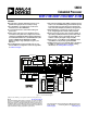
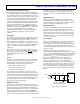
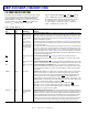
Note that the analog supply pin (A
VDD
) powers the
ADSP-2126x’s internal clock generator PLL. To produce a stable
clock, it is recommended that PCB designs use an external filter
circuit for the A
VDD
pin. Place the filter components as close as
possible to the A
VDD
/A
VSS
pins. For an example circuit, see
Figure 2. (A recommended ferrite chip is the muRata
BLM18AG102SN1D). To reduce noise coupling, the PCB
should use a parallel pair of power and ground planes for
V
DDINT
and GND. Use wide traces to connect the bypass capac-
itors to the analog power (A
VDD
) and ground (A
VSS
) pins. Note
that the A
VDD
and A
VSS
pins specified in Figure 2 are inputs to
the processor and not the analog ground plane on the board—
the A
VSS
pin should connect directly to digital ground (GND) at
the chip.
Figure 2. Analog Power Filter Circuit
HIGH-Z FERRITE
BEAD CHIP
LOCATE ALL COMPONENTS
CLOSE TO A
VDD
AND A
VSS
PINS
A
VDD
A
VSS
100nF 10nF 1nF
ADSP-212xx
V
DDINT