
Datasheet

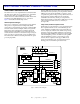

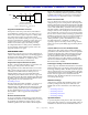
Table Of Contents
- Summary
- Dedicated Audio Components
- Table of Contents
- Revision History
- General Description
- SHARC Family Core Architecture
- SIMD Computational Engine
- Independent, Parallel Computation Units
- Data Register File
- Context Switch
- Universal Registers
- Timer
- Single-Cycle Fetch of Instruction and Four Operands
- Instruction Cache
- Data Address Generators with Zero-Overhead Hardware Circular Buffer Support
- Flexible Instruction Set
- On-Chip Memory
- On-Chip Memory Bandwidth
- ROM-Based Security
- Family Peripheral Architecture
- I/O Processor Features
- System Design
- Development Tools
- Additional Information
- Related Signal Chains
- SHARC Family Core Architecture
- Pin Function Descriptions
- Specifications
- Operating Conditions
- Electrical Characteristics
- Package Information
- ESD Caution
- Maximum Power Dissipation
- Absolute Maximum Ratings
- Timing Specifications
- Core Clock Requirements
- Power-Up Sequencing
- Clock Input
- Clock Signals
- Reset
- Interrupts
- Core Timer
- Timer PWM_OUT Cycle Timing
- Timer WDTH_CAP Timing
- DAI Pin to Pin Direct Routing
- Precision Clock Generator (Direct Pin Routing)
- Flags
- Memory Read—Parallel Port
- Memory Write—Parallel Port
- Serial Ports
- Input Data Port (IDP)
- Parallel Data Acquisition Port (PDAP)
- Pulse-Width Modulation Generators
- Sample Rate Converter—Serial Input Port
- Sample Rate Converter—Serial Output Port
- S/PDIF Transmitter
- S/PDIF Receiver
- SPI Interface—Master
- SPI Interface—Slave
- JTAG Test Access Port and Emulation
- Output Drive Currents
- Test Conditions
- Capacitive Loading
- Thermal Characteristics
- 144-Lead LQFP_EP Pin Configurations
- 136-Ball BGA Pin Configurations
- Package Dimensions
- Automotive Products
- Ordering Guide

Rev. J | Page 4 of 60 | July 2013
ADSP-21362/ADSP-21363/ADSP-21364/ADSP-21365/ADSP-21366
SHARC FAMILY CORE ARCHITECTURE
The ADSP-2136x is code-compatible at the assembly level with
the ADSP-2126x, ADSP-21160, and ADSP-21161, and with the
first generation ADSP-2106x SHARC processors. The
ADSP-2136x shares architectural features with the ADSP-2126x
and ADSP-2116x SIMD SHARC processors, as shown in
Figure 2 and detailed in the following sections.
SIMD Computational Engine
The processor contains two computational processing elements
that operate as a single-instruction, multiple-data (SIMD)
engine. The processing elements are referred to as PEX and PEY
and each contains an ALU, multiplier, shifter, and register file.
PEX is always active, and PEY can be enabled by setting the
PEYEN mode bit in the MODE1 register. When this mode is
enabled, the same instruction is executed in both processing ele-
ments, but each processing element operates on different data.
This architecture is efficient at executing math intensive signal
processing algorithms.
Entering SIMD mode also has an effect on the way data is trans-
ferred between memory and the processing elements. When in
SIMD mode, twice the data bandwidth is required to sustain
computational operation in the processing elements. Because of
this requirement, entering SIMD mode also doubles the
bandwidth between memory and the processing elements.
When using the DAGs to transfer data in SIMD mode, two data
values are transferred with each access of memory or
the register file.
Independent, Parallel Computation Units
Within each processing element is a set of computational units.
The computational units consist of an arithmetic/logic unit
(ALU), multiplier, and shifter. These units perform all opera-
tions in a single cycle. The three units within each processing
element are arranged in parallel, maximizing computational
throughput. Single multifunction instructions execute parallel
ALU and multiplier operations. In SIMD mode, the parallel
ALU and multiplier operations occur in both processing
elements. These computation units support IEEE 32-bit,
single-precision floating-point, 40-bit extended-precision
floating-point, and 32-bit fixed-point data formats.
Figure 2. SHARC Core Block Diagram
S
SIMD Core
CACHEINTERRUPT
5 STAGE
PROGRAM SEQUENCER
PM ADDRESS 32
DM ADDRESS 32
DM DATA 64
PM DATA 64
DAG1
16x32
MRF
80-BIT
ALU
MULTIPLIER
SHIFTER
RF
Rx/Fx
PEx
16x40-BIT
JTAG
DMD/PMD 64
PM DATA 48
ASTATx
STYKx
ASTATy
STYKy
TIMER
RF
Sx/SFx
PEy
16x40-BIT
MRB
80-BIT
MSB
80-BIT
MSF
80-BIT
FLAG
SYSTEM
I/F
USTAT
4x32-BIT
PX
64-BIT
DAG2
16x32
ALU
MULTIPLIER
SHIFTER
DATA
SWAP
PM ADDRESS 24