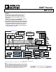
SHARC® Processor ADSP-21371 SUMMARY High performance 32-bit/40-bit floating point processor optimized for high performance audio processing Single-instruction, multiple-data (SIMD) computational architecture On-chip memory—1M bit of on-chip SRAM and a dedicated 4M bit of on-chip mask-programmable ROM Code compatible with all other members of the SHARC family The ADSP-21371 is available with a 266 MHz core instruction rate with unique audiocentric peripherals such as the digi tal applications interface, ser
ADSP-21371 KEY FEATURES—PROCESSOR CORE At 266 MHz (3.75 ns) core instruction rate, the ADSP-21371 performs 1.
ADSP-21371 TABLE OF CONTENTS Summary ................................................................1 Key Features—Processor Core ..................................2 Input/Output Features ............................................2 General Description ..................................................4 ADSP-21371 Family Core Architecture .......................4 ADSP-21371 Memory .............................................5 External Memory ...................................................
ADSP-21371 GENERAL DESCRIPTION The ADSP-21371 SHARC processor is a member of the SIMD SHARC family of DSPs that feature Analog Devices' Super Har vard Architecture. The ADSP-21371 is source code compatible with the ADSP-2126x, ADSP-2136x, and ADSP-2116x DSPs as well as with first generation ADSP-2106x SHARC processors in SISD (single-instruction, single-data) mode.
ADSP-21371 ADSP-21371 MEMORY ments. These computation units support IEEE 32-bit singleprecision floating-point, 40-bit extended precision floatingpoint, and 32-bit fixed-point data formats. The ADSP-21371 adds the following architectural features to the SIMD SHARC family core. Data Register File On-Chip Memory A general-purpose data register file is contained in each pro cessing element. The register files transfer data between the computation units and the data buses, and store intermediate results.
ADSP-21371 Table 2.
ADSP-21371 SDRAM Controller The SDRAM controller provides an interface to up to four sepa rate banks of industry-standard SDRAM devices or DIMMs. Fully compliant with the SDRAM standard, each bank can has its own memory select line (MS0–MS3), and can be configured to contain between 16M bytes and 128M bytes of memory. SDRAM external memory address space is shown in Table 4.
ADSP-21371 Digital Applications Interface (DAI) The digital applications interface (DAI) provides the ability to connect various peripherals to any of the DSP DAI pins (DAI_P20–1). Programs make these connections using the signal routing unit (SRU), shown in Figure 1. The SRU is a matrix routing unit (or group of multiplexers) that enables the peripherals provided by the DAI to be intercon nected under software control.
ADSP-21371 UART Port 2-Wire Interface Port (TWI) The ADSP-21371 processor provides a full-duplex Universal Asynchronous Receiver/Transmitter (UART) port, which is fully compatible with PC-standard UARTs. The UART port provides a simplified UART interface to other peripherals or hosts, supporting full-duplex, DMA-supported, asynchronous transfers of serial data. The UART also has multiprocessor com munication capability using 9-bit address detection.
ADSP-21371 SYSTEM DESIGN The following sections provide an introduction to system design options and power supply issues. Program Booting The internal memory of the ADSP-21371 boots at system power-up from an 8-bit EPROM via the external port, an SPI master, or an SPI slave. Booting is determined by the boot con figuration (BOOTCFG1–0) pins (see Table 7 on Page 14). Selection of the boot source is controlled via the SPI as either a master or slave device, or it can immediately begin executing from ROM.
ADSP-21371 Because the VDK is a library, a developer can decide whether to use it or not. The VDK is integrated into the VisualDSP++ development environment, but can also be used via standard command line tools. When the VDK is used, the development environment assists the developer with many error-prone tasks and assists in managing system resources, automating the gen eration of various VDK based objects, and visualizing the system state, when debugging an application that uses the VDK.
ADSP-21371 PIN FUNCTION DESCRIPTIONS The following symbols appear in the Type column of Table 5: A = asynchronous, I = input, O = output, S = synchronous, (A/D) = active drive, (O/D) = open drain, and T = three-state, (pd) = pull-down resistor, (pu) = pull-up resistor. Table 5.
ADSP-21371 Table 5. Pin List (Continued) Name FLAG[0]/IRQ0 FLAG[1]/IRQ1 FLAG[2]/IRQ2/ MS2 Type I/O I/O I/O with programmable pu (for MS mode) FLAG[3]/TIMEXP/M I/O with S3 programmable pu (for MS mode) TDI I (pu) TDO TMS O /T I (pu) TCK I TRST I (pu) EMU O/T (pu) CLK_CFG1–0 I BOOT_CFG1–0 I RESET I XTAL CLKIN O I CLKOUT/ RESETOUT/ RUNRSTIN I/O (pu) 1 State During and After Reset High-Z/high-Z High-Z/high-Z High-Z/high-Z Description FLAG0/Interrupt Request0. FLAG1/Interrupt Request1.
ADSP-21371 DATA MODES The upper 32 data pins of the external memory interface are muxed (using bits in the SYSCTL register) to support the exter nal memory interface data (input/output), the PDAP (input only), and the FLAGS (input/output). Table 6 provides the pin settings. Table 6.
ADSP-21371 ADSP-21371 SPECIFICATIONS OPERATING CONDITIONS Parameter1 Description Min Max Unit VDDINT VDDEXT VIH2 VIL2 VIH_CLKIN3 VIL_CLKIN3 TJUNCTION Internal (Core) Supply Voltage External (I/O) Supply Voltage High Level Input Voltage @ VDDEXT = max Low Level Input Voltage @ VDDEXT = min High Level Input Voltage @ VDDEXT = max Low Level Input Voltage @ VDDEXT = min Junction Temperature 208-Lead MQFP @ TAMBIENT 0 C to +70 C 1.14 3.13 2.0 –0.5 1.74 –0.5 0 1.26 3.47 VDDEXT + 0.5 +0.8 VDDEXT + 0.5 +1.
ADSP-21371 PACKAGE INFORMATION MAXIMUM POWER DISSIPATION The information presented in Figure 2 provides details about the package branding for the ADSP-21371 processor. For a complete listing of product availability, see Ordering Guide on Page 48. See Engineer-to-Engineer Note “Estimating Power Dissipation for ADSP-2137x SHARC Processors” (EE-319) for detailed thermal and power information regarding maximum power dis sipation.
ADSP-21371 TIMING SPECIFICATIONS Figure 3 shows core to CLKIN ratios of 6:1, 16:1, and 32:1 with external oscillator or crystal. Note that more ratios are possible and can be set through software using the power management control register (PMCTL). For more information, see the ADSP 2136x SHARC Processor Programming Reference. The ADSP-21371’s internal clock (a multiple of CLKIN) pro vides the clock signal for timing internal memory, processor core, and serial ports.
ADSP-21371 Note the definitions of various clock periods shown in Table 12 which are a function of CLKIN and the appropriate ratio con trol shown in Table 11. Table 11. ADSP-21371 CLKOUT and CCLK Clock Generation Operation Timing Requirements CLKIN CCLK Description Input Clock Core Clock Calculation 1/tCK 1/tCCLK Table 12.
ADSP-21371 Power-Up Sequencing The timing requirements for processor startup are given in Table 13. Table 13.
ADSP-21371 Clock Input Table 14. Clock Input Min Parameter Timing Requirements tCK CLKIN Period tCKL CLKIN Width Low tCKH CLKIN Width High tCKRF CLKIN Rise/Fall (0.4 V to 2.0 V) tCCLK3 CCLK Period 22.51 101 101 3.751 1 Applies only for CLKCFG1–0 = 00 and default values for PLL control bits in PMCTL. Applies only for CLKCFG1–0 = 01 and default values for PLL control bits in PMCTL. 3 Any changes to PLL control bits in the PMCTL register must meet core clock timing specification tCCLK.
ADSP-21371 Reset Table 15. Reset Parameter Timing Requirements tWRST1 RESET Pulse Width Low tSRST RESET Setup Before CLKIN Low 1 Min Max 4 tCK 8 Unit ns ns Applies after the power-up sequence is complete. At power-up, the processor’s internal phase-locked loop requires no more than 100 ms while RESET is low, assuming stable VDD and CLKIN (not including start-up time of external clock oscillator). CLKIN tRUNSRST tRUNWRST RESET Figure 7.
ADSP-21371 Interrupts The following timing specification applies to the FLAG0, FLAG1, and FLAG2 pins when they are configured as IRQ0, IRQ1, and IRQ2 interrupts as well as the DAI_P20-1 and DPI_P14-1 pins when they are configured as interrupts. Table 17. Interrupts Parameter Timing Requirement tIPW IRQx Pulse Width DAI_P20-1 DPI_P14-1 FLAG2 -0 (IRQ2-0) Min Max 2 × tPCLK +2 Unit ns tIPW Figure 9.
ADSP-21371 Timer WDTH_CAP Timing The following timing specification applies to timer0, and timer1, and in WDTH_CAP (pulse width count and capture) mode. Timer signals are routed to the DPI_P14–1 pins through the SRU. Therefore, the timing specification provided below is valid at the DPI_P14–1 pins. Table 20. Timer Width Capture Timing Parameter Timing Requirement tPWI Timer Pulse Width Min Max Unit 2 × tPCLK 2 ×(231– 1) × tPCLK ns tPWI DPI_P14-1 (TIMER1-0) Figure 12.
ADSP-21371 Precision Clock Generator (Direct Pin Routing) This timing is only valid when the SRU is configured such that the precision clock generator (PCG) takes its inputs directly from the DAI pins (via pin buffers) and sends its outputs directly to the DAI pins. For the other cases, where the PCG’s inputs and outputs are not directly routed to/from DAI pins (via pin buffers) there is no timing data available.
ADSP-21371 Flags The timing specifications provided below apply to the FLAG3–0 and DPI_P14–1 pins, and the DATA31-0 pins. See Table 5 on page 12 for more information on flag use. Table 23. Flags Parameter Timing Requirement tFIPW DPI_P14-1, DATA31-0, FLAG3–0 IN Pulse Width Switching Characteristic tFOPW DPI_P14-1, DATA31-0, FLAG3–0 OUT Pulse Width Min DPI_P14-1 (FLAG3- 0IN ) (DATA31- 0) tFIPW DPI_P14-1 (FLAG3- 0OUT ) (DATA31- 0) tFOPW Figure 15. Flags Rev.
ADSP-21371 SDRAM Interface Timing (133 MHz SDCLK) Table 24. SDRAM Interface Timing1 Parameter Timing Requirements tSSDAT DATA Setup Before SDCLK tHSDAT DATA Hold After SDCLK Switching Characteristics tSDCLK SDCLK Period tSDCLKH SDCLK Width High tSCCLKL SDCLK Width Low Command, ADDR, Data Delay After SDCLK2 tDCAD tHCAD Command, ADDR, Data Hold After SDCLK2 tDSDAT Data Disable After SDCLK tENSDAT Data Enable After SDCLK 1 2 Min Max 0.58 2.2 ns ns 7.5 3 3 ns ns ns ns ns ns ns 5.3 1.3 5.3 1.
ADSP-21371 Memory Read—Bus Master Use these specifications for asynchronous interfacing to memo ries. Note that timing for ACK, DATA, RD, WR, and strobe timing parameters only apply to asynchronous access mode. Table 25. Memory Read—Bus Master Parameter Min Timing Requirements tDAD Address, Selects Delay to Data Valid1, 2 tDRLD RD Low to Data Valid1 tSDS Data Setup to RD High 2.
ADSP-21371 Memory Write—Bus Master Use these specifications for asynchronous interfacing to memo ries. Note that timing for ACK, DATA, RD, WR, and strobe timing parameters only apply to asynchronous access mode. Table 26. Memory Write—Bus Master Parameter Min Timing Requirements tDAAK ACK Delay from Address, Selects1, 2 tDSAK ACK Delay from WR Low 1, 3 Switching Characteristics tDAWH Address, Selects to WR Deasserted2 tSDCLK – 3.6+ W tDAWL Address, Selects to WR Low2 tSDCLK – 2.7 tWW WR Pulse Width W – 1.
ADSP-21371 Serial Ports To determine whether communication is possible between two devices at clock speed n, the following specifications must be confirmed: 1) frame sync delay and frame sync setup and hold, 2) data delay and data setup and hold, and 3) SCLK width. Serial port signals (SCLK, FS, Data Channel A, Data Channel B) are routed to the DAI_P20–1 pins using the SRU. Therefore, the timing specifications provided below are valid at the DAI_P20–1 pins. Table 27.
ADSP-21371 Table 29. Serial Ports—Enable and Three-State Parameter Switching Characteristics tDDTEN1 Data Enable from External Transmit SCLK Data Disable from External Transmit SCLK tDDTTE1 tDDTIN1 Data Enable from Internal Transmit SCLK 1 Min Max Unit 10 ns ns ns Max Unit 10 ns ns 2 –1 Referenced to drive edge. Table 30.
ADSP-21371 DATA RECEIVE—INTERNAL CLOCK DRIVE EDGE DATA RECEIVE—EXTERNAL CLOCK SAMPLE EDGE DRIVE EDGE SAMPLE EDGE tSCLKIW tSCLKW DAI_P20-1 (SCLK) DAI_P20- 1 (SCLK) tDFSIR tDFSE tHFSI tSFSI tHOFSIR DAI_P20-1 (FS) tHFSE tSFSE tHOFSE DAI_P20-1 (FS) tSDRI tHDRI DAI_P20-1 (DATA CHANNEL A/B) tSDRE tHDRE DAI_P20-1 (DATA CHANNEL A/B) NOTE: EITHER THE RISING EDGE OR FALLING EDGE OF SCLK (EXTERNAL) OR SCLK (INTERNAL) CAN BE USED AS THE ACTIVE SAMPLING EDGE.
ADSP-21371 EXTERNAL RECEIVE FS WITH MCE = 1, MFD = 0 DAI_P20 -1 (SCLK) SAMPLE DRIVE DRIVE tSFSE/I tHFSE/I DAI_P20 -1 (FS) tDDTE/I tDDTENFS tHDTE/I DAI_P20 -1 (DATA CHANNEL A/B) 2ND BIT 1ST BIT tD DTLFSE LATE EXTERNAL TRANSMIT FS DAI_P20-1 (SCLK) SAMPLE DRIVE tSFSE/I DRIVE tHFSE/I DAI_P20 -1 (FS) tDDTE/I tDDTENFS tHDTE/I DAI_P20 -1 (DATA CHANNEL A/B) 1ST BIT 2ND BIT tDDTLFSE NOTE: SERIAL PORT SIGNALS (SCLK, FS, DATA CHANNEL A/B) ARE ROUTED TO THE DAI_P20 -1 PINS USING THE SRU.
ADSP-21371 Input Data Port (IDP) The timing requirements for the IDP are given in Table 31. IDP signals (SCLK, FS, and SDATA) are routed to the DAI_P20–1 pins using the SRU. Therefore, the timing specifications pro vided below are valid at the DAI_P20–1 pins. Table 31.
ADSP-21371 Reference. Note that the most significant 16 bits of external PDAP data can be provided through the DATA31–16 pins. The remaining four bits can only be sourced through DAI_P4–1. The timing below is valid at the DATA31–16 pins. Parallel Data Acquisition Port (PDAP) The timing requirements for the PDAP are provided in Table 32. PDAP is the parallel mode operation of Channel 0 of the IDP.
ADSP-21371 Pulse-Width Modulation Generators (PWM) The following timing specifications apply when the DATA31-16 pins are configured as PWM. Table 33. Pulse-Width Modulation (PWM) Timing Parameter Switching Characteristics tPWMW PWM Output Pulse Width tPWMP PWM Output Period Min Max Unit tPCLK – 2.5 2 × tPCLK – 2.5 (216 – 2) × tPCLK – 2.5 (216 – 1) × tPCLK – 2.5 ns ns tPWMW PWM OUTPUTS tPWMP Figure 23. PWM Timing Rev.
ADSP-21371 S/PDIF Transmitter Serial data input to the S/PDIF transmitter can be formatted as left justified, I2S, or right justified with word widths of 16-, 18-, 20-, or 24-bits. The following sections provide timing for the transmitter. S/PDIF Transmitter-Serial Input Waveforms Figure 24 shows the right-justified mode. LRCLK is high for the left channel and low for the right channel. Data is valid on the rising edge of SCLK.
ADSP-21371 S/PDIF Transmitter Input Data Timing The timing requirements for the S/PDIF transmitter are given in Table 34. Input signals (SCLK, FS, SDATA) are routed to the DAI_P20–1 pins using the SRU. Therefore, the timing specifica tions provided below are valid at the DAI_P20–1 pins. Table 34.
ADSP-21371 S/PDIF Receiver The following section describes timing as it relates to the S/PDIF receiver. Internal Digital PLL Mode In the internal digital phase-locked loop mode the internal PLL (digital PLL) generates the 512 × FS clock. Table 36.
ADSP-21371 SPI Interface—Master The ADSP-21371 contains two SPI ports. Both primary and sec ondary are available through DPI only. The timing provided in Table 37 and Table 38 applies to both. Table 37.
ADSP-21371 SPI Interface—Slave Table 38.
ADSP-21371 Universal Asynchronous Receiver-Transmitter (UART) Port—Receive and Transmit Timing Figure 31 describes UART port receive and transmit operations. The maximum baud rate is PCLK/16 where PCLK = 1/tPCLK. As shown in Figure 31 there is some latency between the genera- tion of internal UART interrupts and the external data operations. These latencies are negligible at the data transmis sion rates for the UART. Table 39.
ADSP-21371 TWI Controller Timing Table 40 and Figure 32 provide timing information for the TWI interface. Input Signals (SCL, SDA) are routed to the DPI_P14–1 pins using the SRU. Therefore, the timing specifica tions provided below are valid at the DPI_P14–1 pins. Table 40. Characteristics of the SDA and SCL Bus Lines for F/S-Mode TWI Bus Devices1 Parameter fSCL tHDSTA tLOW tHIGH tSUSTA tHDDAT tSUDAT tSUSTO tBUF tSP 1 SCL Clock Frequency Hold Time (repeated) Start Condition.
ADSP-21371 JTAG Test Access Port and Emulation Table 41.
ADSP-21371 OUTPUT DRIVE CURRENTS CAPACITIVE LOADING Figure 34 shows typical I-V characteristics for the output driv ers of the ADSP-21371. The curves represent the current drive capability of the output drivers as a function of output voltage. Output delays and holds are based on standard capacitive loads: 30 pF on all pins (see Figure 35). Figure 39 shows graphically how output delays and holds vary with load capacitance.
ADSP-21371 Values of θJB are provided for package comparison and PCB design considerations. Note that the thermal characteristics val ues provided in Table 42 are modeled values. 10 OUTPUT DELAY OR HOLD (ns) 8 Table 42. Thermal Characteristics for 208-Lead MQFP Y = 0.0488X - 1.5923 6 Parameter θJA θJMA θJMA θJC ΨJT ΨJMT ΨJMT 4 2 0 -2 -4 0 50 100 150 200 LOAD CAPACITANCE (pF) Figure 39. Typical Output Delay or Hold vs.
ADSP-21371 208-LEAD MQFP PINOUT Table 43. 208-Lead MQFP Pin Assignment (Numerically by Lead Number) Pin No.
ADSP-21371 Table 43. 208-Lead MQFP Pin Assignment (Numerically by Lead Number) (Continued) Pin No. 45 Signal DATA5 Pin No. 97 Signal ADDR19 Pin No. 149 Signal DAI5 Pin No. 201 46 47 48 49 50 51 52 DATA2 DATA3 DATA0 DATA1 VDDEXT GND VDDINT 98 99 100 101 102 103 104 ADDR20 ADDR21 ADDR23 ADDR22 MS1 MS0 VDD 150 151 152 153 154 155 156 VDDEXT GND VDD GND VDD GND VDD 202 203 204 205 206 207 208 Rev.
ADSP-21371 OUTLINE DIMENSIONS The ADSP-21371 is available in a 208-lead Pb-free MQFP package. 0.75 0.60 0.45 30.60 SQ BSC 4.10 MAX 208 1 SEATING PLANE 157 156 PIN 1 INDICATOR 28.00 SQ BSC TOP VIEW (PINS DOWN) 3.60 3.40 3.20 0.50 0.25 VIEW A 105 104 52 0.20 0.09 53 0.50 BSC 0.08 MAX (LEAD COPLANARITY) (LEAD PITCH) 0.27 0.17 (LEAD WIDTH) VIEW A ROTATED 90° CCW NOTES: 1. THE ACTUAL POSITION OF EACH LEAD IS WITHIN 0.08 FROM ITS IDEAL POSITION WHEN MEASURED IN THE LATERAL DIRECTION. 2.