
Datasheet

ADSP-21371
KEY FEATURES—PROCESSOR CORE
At 266 MHz (3.75 ns) core instruction rate, the ADSP-21371
performs 1.596 GFLOPs/533 MMACs
1M bit on-chip, SRAM for simultaneous access by the core
processor and DMA
4M bit on-chip, mask-programmable ROM
Dual data address generators (DAGs) with modulo and bit-
reverse addressing
Zero-overhead looping with single-cycle loop setup, provid-
ing efficient program sequencing
Single instruction multiple data (SIMD) architecture
provides:
Two computational processing elements
Concurrent execution
Code compatibility with other SHARC family members at
the assembly level
Parallelism in buses and computational units allows:
Single cycle executions (with or without SIMD) of a mul-
tiply operation, an ALU operation, a dual memory read
or write, and an instruction fetch
Transfers between memory and core at a sustained
4.25G bytes/second bandwidth at 266 MHz core instruc-
tion rate
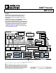
INPUT/OUTPUT FEATURES
DMA controller supports:
32 DMA channels for transfers between ADSP-21371 inter-
nal memory and a variety of peripherals
32-bit DMA transfers at peripheral clock speed, in parallel
with full-speed processor execution
32-bit wide external port provides glueless connection to
both synchronous (SDRAM) and asynchronous memory
devices
Programmable wait state options: 2 to 31 SDCLK cycles
Delay-line DMA engine maintains circular buffers in exter-
nal memory with tap/offset based reads
SDRAM accesses at 133 MHz and asynchronous accesses at
44.4 MHz
4 memory select lines allows multiple external memory
devices
Digital audio interface (DAI) includes eight serial ports, four
precision clock generators, an input data port, an S/PDIF
transceiver, and a signal routing unit
Digital peripheral interface (DPI) includes, two timers, one
UART, and two SPI ports, and a 2-wire interface port
Outputs of PCG’s A and B can be routed through DAI pins
Outputs of PCG's C and D can be driven on to DAI as well as
DPI pins
Eight dual data line serial ports that operate at up to 50 Mbps
on each data line — each has a clock, frame sync, and two
data lines that can be configured as either a receiver or
transmitter pair
TDM support for telecommunications interfaces including
128 TDM channel support for newer telephony interfaces
such as H.100/H.110
Up to 16 TDM stream support, each with 128 channels per
frame
Companding selection on a per channel basis in TDM mode
Input data port, configurable as eight channels of serial data
or seven channels of serial data and up to a 20-bit wide
parallel data channel
Signal routing unit provides configurable and flexible con-
nections between the various peripherals and the DAI/DPI
components
2 muxed flag/IRQ
lines
1 muxed flag/IRQ
/MS pin
1 muxed flag/Timer expired line /MS
pin
S/PDIF-compatible digital audio receiver/transmitter sup-
ports EIAJ CP-340 (CP-1201), IEC-958, AES/EBU standards
Left-justified, I
2
S or right-justified serial data input with
16-, 18-, 20- or 24-bit word widths (transmitter)
Pulse-width modulation provides:
16 PWM outputs configured as four groups of four outputs
supports center-aligned or edge-aligned PWM waveforms
ROM based security features include:
JTAG access to memory permitted with a 64-bit key
Protected memory regions that can be assigned to limit
access under program control to sensitive code
PLL has a wide variety of software and hardware multi-
plier/divider ratios
Newly introduced “Running Reset” feature that allows a reset
of the processor core and peripherals, but without reset-
ting the PLL and SDRAM controller, or performing a boot
Dual voltage: 3.3 V I/O, 1.2 V core
Available in 208-lead MQFP package (see Ordering Guide on
Page 48)
Rev. 0 | Page 2 of 48 | June 2007