
Datasheet

ADSP-21371
GENERAL DESCRIPTION
The ADSP-21371 SHARC processor is a member of the SIMD
SHARC family of DSPs that feature Analog Devices' Super Har-
vard Architecture. The ADSP-21371 is source code compatible
with the ADSP-2126x, ADSP-2136x, and ADSP-2116x DSPs as
well as with first generation ADSP-2106x SHARC processors in
SISD (single-instruction, single-data) mode. The ADSP-21371
is a 32-bit/40-bit floating point processors optimized for high
performance automotive audio applications with its large on-
chip SRAM and mask-programmable ROM, multiple internal
buses to eliminate I/O bottlenecks, and an innovative digital
applications interface (DAI).
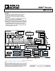
As shown in the functional block diagram on Page 1, the
ADSP-21371 uses two computational units to deliver a signifi-
cant performance increase over the previous SHARC processors
on a range of DSP algorithms. Fabricated in a state-of-the-art,
high speed, CMOS process, the ADSP-21371 processor achieves
an instruction cycle time of 3.75 ns at 266 MHz. With its SIMD
computational hardware, the ADSP-21371 can perform
1.596 GFLOPS running at 266 MHz.
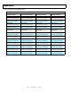
Table 1 shows performance benchmarks for the ADSP-21371.
Table 1. ADSP-21371 Benchmarks (at 266 MHz)
Benchmark Algorithm
1024 Point Complex FFT (Radix 4, With Reversal)
FIR Filter (per Tap)
1
IIR Filter (per Biquad)
1
Matrix Multiply (Pipelined)
[3 3] × [3 1]
[4 4] × [4 1]
Divide (y/×)
Inverse Square Root
Speed
(at 266 MHz)
34.5 μs
1.88 ns
7.5 ns
16.91 ns
30.07 ns
13.1 ns
20.4 ns
1
Assumes two files in multichannel SIMD mode
The ADSP-21371 continues SHARC’s industry-leading stan-
dards of integration for DSPs, combining a high performance
32-bit DSP core with integrated, on-chip system features.
The block diagram of the ADSP-21371 on Page 1 illustrates the
following architectural features:
• Two processing elements, each of which comprises an
ALU, multiplier, shifter, and data register file
• Data address generators (DAG1, DAG2)
• Program sequencer with instruction cache
• PM and DM buses capable of supporting four 32-bit data
transfers between memory and the core at every core pro-
cessor cycle
• Two programmable interval timers with external event
counter capabilities
•On-chip SRAM (1M bit)
•On-chip mask-programmable ROM (4M bit)
• JTAG test access port
The block diagram of the ADSP-21371 on Page 1 also illustrates
the following architectural features:
• DMA controller
• Digital applications interface that includes four precision
clock generators (PCG), an S/PDIF-compatible digital
audio receiver/transmitter, an input data port (IDP), eight
serial ports, eight serial interfaces, a 20-bit parallel input
port (PDAP), and a flexible signal routing unit (DAI SRU).
• Digital peripheral interface that includes two timers, one
UART, two serial peripheral interfaces (SPI), a 2-wire
interface (TWI), and a flexible signal routing unit
(DPI SRU).
ADSP-21371 FAMILY CORE ARCHITECTURE
The ADSP-21371 is code compatible at the assembly level with
the ADSP-21375, ADSP-2136x, ADSP-2126x, ADSP-21160, and
ADSP-21161, and with the first generation ADSP-2106x
SHARC processors. The ADSP-21371 shares architectural fea-
tures with the ADSP-2126x, ADSP-2136x, and ADSP-2116x
SIMD SHARC processors, as detailed in the following sections.
SIMD Computational Engine
The ADSP-21371 contains two computational processing ele-
ments that operate as a single-instruction, multiple-data
(SIMD) engine. The processing elements are referred to as PEX
and PEY and each contains an ALU, multiplier, shifter, and reg-
ister file. PEX is always active, and PEY may be enabled by
setting the PEYEN mode bit in the MODE1 register. When this
mode is enabled, the same instruction is executed in both pro-
cessing elements, but each processing element operates on
different data. This architecture is efficient at executing math
intensive DSP algorithms.
Entering SIMD mode also has an effect on the way data is trans-
ferred between memory and the processing elements. When in
SIMD mode, twice the data bandwidth is required to sustain
computational operation in the processing elements. Because of
this requirement, entering SIMD mode also doubles the band-
width between memory and the processing elements. When
using the DAGs to transfer data in SIMD mode, two data values
are transferred with each access of memory or the register file.
Independent, Parallel Computation Units
Within each processing element is a set of computational units.
The computational units consist of an arithmetic/logic unit
(ALU), multiplier, and shifter. These units perform all opera-
tions in a single cycle. The three units within each processing
element are arranged in parallel, maximizing computational
throughput. Single multifunction instructions execute parallel
ALU and multiplier operations. In SIMD mode, the parallel
ALU and multiplier operations occur in both processing ele-
Rev. 0 | Page 4 of 48 | June 2007