SHARC Processor ADSP-21483/ADSP-21486/ADSP-21487/ADSP-21488/ADSP-21489 SUMMARY The ADSP-2148x processors are available with unique audiocentric peripherals, such as the digital applications interface, serial ports, precision clock generators, S/PDIF transceiver, asynchronous sample rate converters, input data port, and more For complete ordering information, see Ordering Guide on Page 66 High performance 32-bit/40-bit floating-point processor optimized for high performance audio processing Single-instructi
ADSP-21483/ADSP-21486/ADSP-21487/ADSP-21488/ADSP-21489 TABLE OF CONTENTS Summary ............................................................... 1 Maximum Power Dissipation ................................. 21 General Description ................................................. 3 Package Information ............................................ 21 Family Core Architecture ........................................ 4 Timing Specifications ...........................................
ADSP-21483/ADSP-21486/ADSP-21487/ADSP-21488/ADSP-21489 GENERAL DESCRIPTION The ADSP-2148x SHARC® processors are members of the SIMD SHARC family of DSPs that feature Analog Devices’ Super Harvard Architecture. The processors are source code compatible with the ADSP-2126x, ADSP-2136x, ADSP-2137x, ADSP-2146x, ADSP-2147x and ADSP-2116x DSPs, as well as with first generation ADSP-2106x SHARC processors in SISD (single-instruction, single-data) mode.
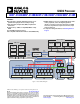
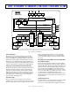
ADSP-21483/ADSP-21486/ADSP-21487/ADSP-21488/ADSP-21489 The diagram on Page 1 shows the two clock domains that make up the ADSP-2148x processors.
ADSP-21483/ADSP-21486/ADSP-21487/ADSP-21488/ADSP-21489 S JTAG FLAG TIMER INTERRUPT CACHE SIMD Core PM ADDRESS 24 DMD/PMD 64 5 STAGE PROGRAM SEQUENCER PM DATA 48 DAG1 16x32 DAG2 16x32 PM ADDRESS 32 SYSTEM I/F DM ADDRESS 32 USTAT 4x32-BIT PM DATA 64 PX 64-BIT DM DATA 64 MULTIPLIER MRF 80-BIT MRB 80-BIT SHIFTER ALU RF Rx/Fx PEx 16x40-BIT DATA SWAP RF Sx/SFx PEy 16x40-BIT ASTATx ASTATy STYKx STYKy ALU SHIFTER MULTIPLIER MSB 80-BIT MSF 80-BIT Figure 2.
ADSP-21483/ADSP-21486/ADSP-21487/ADSP-21488/ADSP-21489 subtract in both processing elements while branching and fetching up to four 32-bit values from memory, all in a single instruction. Variable Instruction Set Architecture (VISA) In addition to supporting the standard 48-bit instructions from previous SHARC processors, the ADSP-2148x supports new instructions of 16 and 32 bits.
ADSP-21483/ADSP-21486/ADSP-21487/ADSP-21488/ADSP-21489 Table 4.
ADSP-21483/ADSP-21486/ADSP-21487/ADSP-21488/ADSP-21489 • Arbitration logic to coordinate core and DMA transfers between internal and external memory over the external port. A set of programmable timing parameters is available to configure the SDRAM banks to support slower memory devices. Note that 32-bit wide devices are not supported on the SDRAM and AMI interfaces. Non-SDRAM external memory address space is shown in Table 5.
ADSP-21483/ADSP-21486/ADSP-21487/ADSP-21488/ADSP-21489 The PWM generator is capable of operating in two distinct modes while generating center-aligned PWM waveforms: single-update mode or double-update mode. In single-update mode the duty cycle values are programmable only once per PWM period. This results in PWM patterns that are symmetrical about the midpoint of the PWM period. In double-update mode, a second updating of the PWM registers is implemented at the midpoint of the PWM period.
ADSP-21483/ADSP-21486/ADSP-21487/ADSP-21488/ADSP-21489 The outputs of PCG A and B can be routed through the DAI pins and the outputs of PCG C and D can be driven on to the DAI as well as the DPI pins.
ADSP-21483/ADSP-21486/ADSP-21487/ADSP-21488/ADSP-21489 Table 9. Boot Mode Selection, 176-Lead Package Delay Line DMA The processor provides delay line DMA functionality. This allows processor reads and writes to external delay line buffers (and hence to external memory) with limited core interaction. Scatter/Gather DMA The processor provides scatter/gather DMA functionality. This allows processor DMA reads/writes to/from non contiguous memory blocks.
ADSP-21483/ADSP-21486/ADSP-21487/ADSP-21488/ADSP-21489 Details on power consumption and Static and Dynamic current consumption can be found at Total Power Dissipation on Page 20. Also see Operating Conditions on Page 18 for more information. The following are SVS features. • SVS is applicable only to 450 MHz models (not applicable to 400 MHz or lower frequency models). • Each individual SVS device includes a register (SVS_DAT) containing the unique SVS voltage set at the factory, known as SVSNOM.
ADSP-21483/ADSP-21486/ADSP-21487/ADSP-21488/ADSP-21489 Analog Devices eases signal processing system development by providing signal processing components that are designed to work together well. A tool for viewing relationships between specific applications and related components is available on the www.analog.com website. Middleware Packages Analog Devices separately offers middleware add-ins such as real time operating systems, file systems, USB stacks, and TCP/IP stacks.
ADSP-21483/ADSP-21486/ADSP-21487/ADSP-21488/ADSP-21489 PIN FUNCTION DESCRIPTIONS Table 11. Pin Descriptions Name ADDR23–0 Type I/O/T (ipu) State During/ After Reset High-Z/ driven low (boot) DATA15–0 I/O/T (ipu) High-Z AMI_ACK I (ipu) MS0–1 O/T (ipu) High-Z AMI_RD O/T (ipu) High-Z AMI_WR O/T (ipu) High-Z FLAG[0] INPUT FLAG1/IRQ1 I/O (ipu) FLAG[1] FLAG1/Interrupt Request1. INPUT FLAG2/IRQ2/MS2 I/O (ipu) FLAG[2] FLAG2/Interrupt Request2/Memory Select2.
ADSP-21483/ADSP-21486/ADSP-21487/ADSP-21488/ADSP-21489 Table 11. Pin Descriptions (Continued) Name SDRAS Type O/T (ipu) State During/ After Reset High-Z/ driven high High-Z/ driven high High-Z/ driven high Description SDRAM Row Address Strobe. Connect to SDRAM’s RAS pin. In conjunction with other SDRAM command pins, defines the operation for the SDRAM to perform. SDCAS O/T (ipu) SDRAM Column Address Select. Connect to SDRAM’s CAS pin.
ADSP-21483/ADSP-21486/ADSP-21487/ADSP-21488/ADSP-21489 Table 11. Pin Descriptions (Continued) Name MLBCLK1 Type I State During/ After Reset Description Media Local Bus Clock. This clock is generated by the MLB controller that is synchronized to the MOST network and provides the timing for the entire MLB interface at 49.152 MHz at FS=48 kHz. When the MLB controller is not used, this pin should be grounded. 1 I/O/T in 3 High-Z Media Local Bus Data.
ADSP-21483/ADSP-21486/ADSP-21487/ADSP-21488/ADSP-21489 Table 11. Pin Descriptions (Continued) Name CLK_CFG1–0 Description Core to CLKIN Ratio Control. These pins set the start up clock frequency. Note that the operating frequency can be changed by programming the PLL multiplier and divider in the PMCTL register at any time after the core comes out of reset. The allowed values are: 00 = 8:1 01 = 32:1 10 = 16:1 11 = reserved CLKIN I Local Clock In. Used in conjunction with XTAL. CLKIN is the clock input.
ADSP-21483/ADSP-21486/ADSP-21487/ADSP-21488/ADSP-21489 SPECIFICATIONS OPERATING CONDITIONS 300 MHz / 350 MHz / 400 MHz Parameter1 Description VDD_INT 2 Internal (Core) Supply Voltage 450 MHz Min Nom Max Min Nom Max Unit 1.05 1.1 1.15 SVSNOM – 25 mV 1.0 – 1.15 SVSNOM + 25 mV V VDD_EXT External (I/O) Supply Voltage 3.13 3.47 3.13 3.47 V VDD_THD Thermal Diode Supply Voltage 3.13 3.47 3.13 3.47 V VIH3 High Level Input Voltage @ VDD_EXT = Max 2.0 3.6 2.0 3.
ADSP-21483/ADSP-21486/ADSP-21487/ADSP-21488/ADSP-21489 ELECTRICAL CHARACTERISTICS 300 MHz / 350 MHz / 400 MHz / 450 MHz Parameter1 Description 2 Test Conditions Min 2.4 VOH High Level Output Voltage @ VDD_EXT = Min, IOH = –1.0 mA3 VOL2 Low Level Output Voltage @ VDD_EXT = Min, IOL = 1.0 mA3 IIH4, 5 IIL4 Typ Max Unit V 0.
ADSP-21483/ADSP-21486/ADSP-21487/ADSP-21488/ADSP-21489 Total Power Dissipation The information in this section should be augmented with the Engineer-to-Engineer Note “Estimating Power for ADSP-214xx SHARC Processors” (EE-348). Table 13. Activity Scaling Factors (ASF)1 Activity Idle Low Medium Low Medium High Peak Typical (50:50)2 Peak Typical (60:40)2 Peak Typical (70:30)2 High Typical High Peak Total power dissipation has two components: 1.
ADSP-21483/ADSP-21486/ADSP-21487/ADSP-21488/ADSP-21489 Table 15. Dynamic Current in CCLK Domain—IDD_INT_DYNAMIC (mA, with ASF = 1.0)1, 2 fCCLK (MHz) 100 150 200 250 300 350 400 450 1 2 VDD_INT (V) 0.975 V 76 117 153 190 227 263 300 339 1.0 V 77 119 156 195 233 272 309 349 1.025 V 81 123 161 201 240 278 317 356 1.05 V 84 126 165 207 246 286 326 365 1.075 V 87 130 170 212 253 294 335 374 1.10 V 88 133 174 217 260 302 344 385 1.125 V 90 136 179 223 266 309 352 394 1.
ADSP-21483/ADSP-21486/ADSP-21487/ADSP-21488/ADSP-21489 TIMING SPECIFICATIONS Timing Requirements apply to signals that are controlled by circuitry external to the processor, such as the data input for a read operation. Timing requirements guarantee that the processor operates correctly with other devices. Use the exact timing information given. Do not attempt to derive parameters from the addition or subtraction of others.
ADSP-21483/ADSP-21486/ADSP-21487/ADSP-21488/ADSP-21489 Note the definitions of the clock periods that are a function of CLKIN and the appropriate ratio control shown in Table 18. All of the timing specifications for the ADSP-2148x peripherals are defined in relation to tPCLK. See the peripheral specific section for each peripheral’s timing information. Power-Up Sequencing The timing requirements for processor startup are given in Table 19.
ADSP-21483/ADSP-21486/ADSP-21487/ADSP-21488/ADSP-21489 RESET tRSTVDD VDDINT tIVDDEVDD VDDEXT tCLKVDD CLKIN tCLKRST CLK_CFG1–0 tPLLRST tCORERST RESETOUT Figure 5. Power-Up Sequencing Clock Input Table 20. Clock Input Parameter Timing Requirements tCK CLKIN Period tCKL CLKIN Width Low CLKIN Width High tCKH tCKRF3 CLKIN Rise/Fall (0.4 V to 2.0 V) tCCLK4 CCLK Period fVCO5 VCO Frequency tCKJ6, 7 CLKIN Jitter Tolerance 300 MHz Min Max 350 MHz Min Max 400 MHz Min Max 450 MHz Min Max 26.
ADSP-21483/ADSP-21486/ADSP-21487/ADSP-21488/ADSP-21489 Clock Signals The ADSP-2148x can use an external clock or a crystal. See the CLKIN pin description in Table 11 on Page 14. Programs can configure the processor to use its internal clock generator by connecting the necessary components to CLKIN and XTAL. Figure 7 shows the component connections used for a crystal operating in fundamental mode.
ADSP-21483/ADSP-21486/ADSP-21487/ADSP-21488/ADSP-21489 Reset Table 21. Reset Parameter Timing Requirements tWRST1 RESET Pulse Width Low tSRST RESET Setup Before CLKIN Low 1 Min Max 4 × tCK 8 Unit ns ns Applies after the power-up sequence is complete. At power-up, the processor’s internal phase-locked loop requires no more than 100 μ while RESET is low, assuming stable VDD and CLKIN (not including start-up time of external clock oscillator). CLKIN tWRST tSRST RESET Figure 8.
ADSP-21483/ADSP-21486/ADSP-21487/ADSP-21488/ADSP-21489 Interrupts The following timing specification applies to the FLAG0, FLAG1, and FLAG2 pins when they are configured as IRQ0, IRQ1, and IRQ2 interrupts, as well as the DAI_P20–1 and DPI_P14–1 pins when they are configured as interrupts. Table 23. Interrupts Parameter Timing Requirement tIPW IRQx Pulse Width Min Max 2 × tPCLK +2 Unit ns INTERRUPT INPUTS tIPW Figure 10.
ADSP-21483/ADSP-21486/ADSP-21487/ADSP-21488/ADSP-21489 Timer PWM_OUT Cycle Timing The following timing specification applies to timer0 and timer1 in PWM_OUT (pulse-width modulation) mode. Timer signals are routed to the DPI_P14–1 pins through the DPI SRU. Therefore, the timing specifications provided below are valid at the DPI_P14–1 pins. Table 25. Timer PWM_OUT Timing Parameter Switching Characteristic tPWMO Timer Pulse Width Output Min Max Unit 2 × tPCLK – 1.
ADSP-21483/ADSP-21486/ADSP-21487/ADSP-21488/ADSP-21489 Watchdog Timer Timing Table 27. Watchdog Timer Timing Parameter Timing Requirement tWDTCLKPER Switching Characteristics tRST WDT Clock Rising Edge to Watchdog Timer RESET Falling Edge tRSTPW Reset Pulse Width Min Max Unit 100 1000 ns 3 6.4 ns 64 × tWDTCLKPER ns tWDTCLKPER WDT_CLKIN tRST tRSTPW WDTRSTO Figure 14.
ADSP-21483/ADSP-21486/ADSP-21487/ADSP-21488/ADSP-21489 Precision Clock Generator (Direct Pin Routing) This timing is only valid when the SRU is configured such that the precision clock generator (PCG) takes its inputs directly from the DAI pins (via pin buffers) and sends its outputs directly to the DAI pins. For the other cases, where the PCG’s inputs and outputs are not directly routed to/from DAI pins (via pin buffers), there is no timing data available.
ADSP-21483/ADSP-21486/ADSP-21487/ADSP-21488/ADSP-21489 Flags The timing specifications provided below apply to the DPI_P14–1, ADDR7–0, ADDR23–8, DATA7–0, and FLAG3–0 pins when configured as FLAGS. See Table 11 on Page 14 for more information on flag use. Table 30. Flags Parameter Timing Requirement tFIPW1 FLAGs IN Pulse Width Switching Characteristic FLAGs OUT Pulse Width tFOPW1 1 Min tFIPW FLAG OUTPUTS tFOPW Figure 17. Flags Rev.
ADSP-21483/ADSP-21486/ADSP-21487/ADSP-21488/ADSP-21489 SDRAM Interface Timing (166 MHz SDCLK) The maximum frequency for SDRAM is 166 MHz. For information on SDRAM frequency and programming, see the ADSP-214xx SHARC Processor Hardware Reference, Engineerto-Engineer Note “Interfacing SDRAM Memories to SHARC Processors” (EE-286), and the SDRAM vendor data sheet. Table 31.
ADSP-21483/ADSP-21486/ADSP-21487/ADSP-21488/ADSP-21489 AMI Read Use these specifications for asynchronous interfacing to memories. Note that timing for AMI_ACK, ADDR, DATA, AMI_RD, AMI_WR, and strobe timing parameters only apply to asynchronous access mode. Table 32. AMI Read Parameter Min Timing Requirements tDAD1, 2, 3 Address Selects Delay to Data Valid 1, 3 tDRLD AMI_RD Low to Data Valid Data Setup to AMI_RD High 2.
ADSP-21483/ADSP-21486/ADSP-21487/ADSP-21488/ADSP-21489 AMI_ADDR AMI_MSx tDARL tRW tDRHA AMI_RD tDRLD tSDS tDAD tHDRH AMI_DATA tRWR tDSAK tDAAK AMI_ACK AMI_WR Figure 19. AMI Read Rev.
ADSP-21483/ADSP-21486/ADSP-21487/ADSP-21488/ADSP-21489 AMI Write Use these specifications for asynchronous interfacing to memories. Note that timing for AMI_ACK, ADDR, DATA, AMI_RD, AMI_WR, and strobe timing parameters only apply to asynchronous access mode. Table 33. AMI Write Parameter Min Timing Requirements tDAAK1, 2 AMI_ACK Delay from Address, Selects 1, 3 tDSAK AMI_ACK Delay from AMI_WR Low Switching Characteristics tDAWH2 Address Selects to AMI_WR Deasserted tSDCLK – 3.
ADSP-21483/ADSP-21486/ADSP-21487/ADSP-21488/ADSP-21489 Serial Ports In slave transmitter mode and master receiver mode, the maximum serial port frequency is fPCLK/8. In master transmitter mode and slave receiver mode, the maximum serial port clock frequency is fPCLK/4. To determine whether communication is possible between two devices at clock speed n, the following specifications must be confirmed: 1) frame sync delay and frame sync setup and hold; 2) data delay and data setup and hold; and 3) SCLK width.
ADSP-21483/ADSP-21486/ADSP-21487/ADSP-21488/ADSP-21489 DATA RECEIVE—INTERNAL CLOCK DRIVE EDGE tSCLKIW DATA RECEIVE—EXTERNAL CLOCK SAMPLE EDGE DRIVE EDGE DAI_P20–1 (SCLK) SAMPLE EDGE tSCLKW DAI_P20–1 (SCLK) tDFSI tDFSE tSFSI tHOFSI tHFSI DAI_P20–1 (FS) tSFSE tHFSE tSDRE tHDRE tHOFSE DAI_P20–1 (FS) tSDRI tHDRI DAI_P20–1 (DATA CHANNEL A/B) DAI_P20–1 (DATA CHANNEL A/B) DATA TRANSMIT—INTERNAL CLOCK DRIVE EDGE tSCLKIW DATA TRANSMIT—EXTERNAL CLOCK SAMPLE EDGE DRIVE EDGE DAI_P20–1 (SCLK)
ADSP-21483/ADSP-21486/ADSP-21487/ADSP-21488/ADSP-21489 Table 36. Serial Ports—External Late Frame Sync Parameter Switching Characteristics tDDTLFSE1 Data Delay from Late External Transmit Frame Sync or External Receive Frame Sync with MCE = 1, MFD = 0 tDDTENFS1 Data Enable for MCE = 1, MFD = 0 1 Min Max 8.5 ns ns 0.5 The tDDTLFSE and tDDTENFS parameters apply to left-justified, as well as DSP serial mode, and MCE = 1, MFD = 0.
ADSP-21483/ADSP-21486/ADSP-21487/ADSP-21488/ADSP-21489 Table 37. Serial Ports—Enable and Three-State Parameter Switching Characteristics tDDTEN1 Data Enable from External Transmit SCLK Data Disable from External Transmit SCLK tDDTTE1 tDDTIN1 Data Enable from Internal Transmit SCLK 1 Min Max Unit 11.5 ns ns ns 2 –1.5 Referenced to drive edge.
ADSP-21483/ADSP-21486/ADSP-21487/ADSP-21488/ADSP-21489 The SPORTx_TDV_O output signal (routing unit) becomes active in SPORT multichannel mode. During transmit slots (enabled with active channel selection registers) the SPORTx_TDV_O is asserted for communication with external devices. Table 38.
ADSP-21483/ADSP-21486/ADSP-21487/ADSP-21488/ADSP-21489 Input Data Port (IDP) The timing requirements for the IDP are given in Table 39. IDP signals are routed to the DAI_P20–1 pins using the SRU. Therefore, the timing specifications provided below are valid at the DAI_P20–1 pins. Table 39.
ADSP-21483/ADSP-21486/ADSP-21487/ADSP-21488/ADSP-21489 PDAP chapter of the ADSP-214xx SHARC Processor Hardware Reference. Note that the 20 bits of external PDAP data can be provided through the ADDR23–4 pins or over the DAI pins. Parallel Data Acquisition Port (PDAP) The timing requirements for the PDAP are provided in Table 40. PDAP is the parallel mode operation of Channel 0 of the IDP. For details on the operation of the PDAP, see the Table 40.
ADSP-21483/ADSP-21486/ADSP-21487/ADSP-21488/ADSP-21489 Sample Rate Converter—Serial Input Port The ASRC input signals are routed from the DAI_P20–1 pins using the SRU. Therefore, the timing specifications provided in Table 41 are valid at the DAI_P20–1 pins. Table 41.
ADSP-21483/ADSP-21486/ADSP-21487/ADSP-21488/ADSP-21489 specification with regard to serial clock. Note that serial clock rising edge is the sampling edge, and the falling edge is the drive edge. Sample Rate Converter—Serial Output Port For the serial output port, the frame sync is an input, and it should meet setup and hold times with regard to SCLK on the output port. The serial data output has a hold time and delay Table 42.
ADSP-21483/ADSP-21486/ADSP-21487/ADSP-21488/ADSP-21489 Pulse-Width Modulation Generators (PWM) The following timing specifications apply when the ADDR23–8/DPI_14–1 pins are configured as PWM. Table 43. Pulse-Width Modulation (PWM) Timing Parameter Switching Characteristics tPWMW PWM Output Pulse Width tPWMP PWM Output Period Min Max Unit tPCLK – 2 2 × tPCLK – 1.5 (216 – 2) × tPCLK (216 – 1) × tPCLK ns ns tPWMW PWM OUTPUTS tPWMP Figure 29.
ADSP-21483/ADSP-21486/ADSP-21487/ADSP-21488/ADSP-21489 Figure 31 shows the default I2S-justified mode. The frame sync is low for the left channel and HI for the right channel. Data is valid on the rising edge of serial clock. The MSB is left-justified to the frame sync transition but with a delay. Table 45.
ADSP-21483/ADSP-21486/ADSP-21487/ADSP-21488/ADSP-21489 S/PDIF Transmitter Input Data Timing The timing requirements for the S/PDIF transmitter are given in Table 47. Input signals are routed to the DAI_P20–1 pins using the SRU. Therefore, the timing specifications provided below are valid at the DAI_P20–1 pins. Table 47.
ADSP-21483/ADSP-21486/ADSP-21487/ADSP-21488/ADSP-21489 S/PDIF Receiver The following section describes timing as it relates to the S/PDIF receiver. Internal Digital PLL Mode In the internal digital phase-locked loop mode the internal PLL (digital PLL) generates the 512 × FS clock. Table 49.
ADSP-21483/ADSP-21486/ADSP-21487/ADSP-21488/ADSP-21489 SPI Interface—Master The ADSP-2148x contains two SPI ports. Both primary and secondary are available through DPI only. The timing provided in Table 50 and Table 51 applies to both. Table 50.
ADSP-21483/ADSP-21486/ADSP-21487/ADSP-21488/ADSP-21489 SPI Interface—Slave Table 51.
ADSP-21483/ADSP-21486/ADSP-21487/ADSP-21488/ADSP-21489 Media Local Bus All the numbers given are applicable for all speed modes (1024 FS, 512 FS and 256 FS for 3-pin; 512 FS and 256 FS for 5-pin), unless otherwise specified. Please refer to the MediaLB specification document revision 3.0 for more details. Table 52.
ADSP-21483/ADSP-21486/ADSP-21487/ADSP-21488/ADSP-21489 MLBSIG/ MLBDAT (Rx, Input) VALID tDHMCF tDSMCF tMCKH MLBCLK tMCKR tMCKL tMCKF tMLBCLK tMCFDZ tMCDRV tMDZH MLBSIG/ MLBDAT (Tx, Output) VALID Figure 37. MLB Timing (3-Pin Interface) Table 53.
ADSP-21483/ADSP-21486/ADSP-21487/ADSP-21488/ADSP-21489 MLBSIG/ MLBDAT (Rx, Input) VALID tDHMCF tDSMCF tMCKH MLBCLK tMCKR tMCKL tMCKF tMLBCLK tMCRDL tMCDRV VALID MLBSO/ MLBDO (Tx, Output) Figure 38. MLB Timing (5-Pin Interface) MLBCLK tMPWV tMPWV Figure 39.
ADSP-21483/ADSP-21486/ADSP-21487/ADSP-21488/ADSP-21489 JTAG Test Access Port and Emulation Table 54.
ADSP-21483/ADSP-21486/ADSP-21487/ADSP-21488/ADSP-21489 OUTPUT DRIVE CURRENTS TESTER PIN ELECTRONICS Figure 41 shows typical I-V characteristics for the output drivers of the ADSP-2148x, and Table 55 shows the pins associated with each driver. The curves represent the current drive capability of the output drivers as a function of output voltage. 50: VLOAD T1 70: ZO = 50: (impedance) TD = 4.04 r 1.18 ns 50: Table 55. Driver Types 0.
ADSP-21483/ADSP-21486/ADSP-21487/ADSP-21488/ADSP-21489 9 14 8 TYPE A DRIVE FALL y = 0.0747x + 0.5154 10 RISE AND FALL TIMES DELAY (ns) RISE AND FALL TIMES (ns) 12 TYPE A DRIVE RISE y = 0.0571x + 0.5558 8 TYPE B DRIVE FALL y = 0.0278x + 0.3138 6 4 TYPE B DRIVE RISE y = 0.0258x + 0.3684 2 TYPE A DRIVE RISE y = 0.0256x + 3.5859 TYPE A DRIVE FALL y = 0.0359x + 2.924 7 TYPE B DRIVE RISE y = 0.0116x + 3.5697 6 5 4 3 TYPE B DRIVE FALL y = 0.0136x + 3.
ADSP-21483/ADSP-21486/ADSP-21487/ADSP-21488/ADSP-21489 Note that the thermal characteristics values provided in Table 56 and Table 57 are modeled values. Thermal Diode The ADSP-2148x processors incorporate thermal diode/s to monitor the die temperature. The thermal diode of is a grounded collector, PNP Bipolar Junction Transistor (BJT). The THD_P pin is connected to the emitter and the THD_M pin is connected to the base of the transistor.
ADSP-21483/ADSP-21486/ADSP-21487/ADSP-21488/ADSP-21489 100-LQFP_EP LEAD ASSIGNMENT Table 59. 100-Lead LQFP_EP Lead Assignments (Numerical by Lead Number) Lead Name VDD_INT CLK_CFG1 BOOT_CFG0 VDD_EXT VDD_INT BOOT_CFG1 GND NC NC CLK_CFG0 VDD_INT CLKIN XTAL VDD_EXT VDD_INT VDD_INT RESETOUT/RUNRSTIN VDD_INT DPI_P01 DPI_P02 DPI_P03 VDD_INT DPI_P05 DPI_P04 DPI_P06 Lead No.
ADSP-21483/ADSP-21486/ADSP-21487/ADSP-21488/ADSP-21489 Figure 48 shows the top view of the 100-lead LQFP_EP lead configuration. Figure 49 shows the bottom view of the 100-lead LQFP_EP lead configuration. LEAD 100 LEAD 76 LEAD 1 LEAD 75 LEAD 1 INDICATOR ADSP-2148x 100-LEAD LQFP_EP TOP VIEW LEAD 25 LEAD 51 LEAD 26 LEAD 50 Figure 48.
ADSP-21483/ADSP-21486/ADSP-21487/ADSP-21488/ADSP-21489 176-LEAD LQFP_EP LEAD ASSIGNMENT Table 60. ADSP-21486 176-Lead LQFP_EP Lead Assignment (Numerical by Lead Number) Lead Name NC MS0 NC VDD_INT CLK_CFG1 ADDR0 BOOT_CFG0 VDD_EXT ADDR1 ADDR2 ADDR3 ADDR4 ADDR5 BOOT_CFG1 GND ADDR6 ADDR7 NC NC ADDR8 ADDR9 CLK_CFG0 VDD_INT CLKIN XTAL ADDR10 NC VDD_EXT VDD_INT ADDR11 ADDR12 ADDR17 ADDR13 VDD_INT ADDR18 RESETOUT/RUNRSTIN VDD_INT DPI_P01 DPI_P02 DPI_P03 VDD_INT DPI_P05 DPI_P04 DPI_P06 Lead No.
ADSP-21483/ADSP-21486/ADSP-21487/ADSP-21488/ADSP-21489 Table 61. ADSP-21483, ADSP-21487, ADSP-21488, and ADSP-21489 176-Lead LQFP_EP Lead Assignment (Numerical by Lead Number) Lead Name SDDQM MS0 SDCKE VDD_INT CLK_CFG1 ADDR0 BOOT_CFG0 VDD_EXT ADDR1 ADDR2 ADDR3 ADDR4 ADDR5 BOOT_CFG1 GND ADDR6 ADDR7 NC NC ADDR8 ADDR9 CLK_CFG0 VDD_INT CLKIN XTAL ADDR10 SDA10 VDD_EXT VDD_INT ADDR11 ADDR12 ADDR17 ADDR13 VDD_INT ADDR18 RESETOUT/RUNRSTIN VDD_INT DPI_P01 DPI_P02 DPI_P03 VDD_INT DPI_P05 DPI_P04 DPI_P06 Lead No.
ADSP-21483/ADSP-21486/ADSP-21487/ADSP-21488/ADSP-21489 Table 62. Automotive Models ADSP-21488, and ADSP-21489 176-Lead LQFP_EP Lead Assignment (Numerical by Lead Number) Lead Name SDDQM MS0 SDCKE VDD_INT CLK_CFG1 ADDR0 BOOT_CFG0 VDD_EXT ADDR1 ADDR2 ADDR3 ADDR4 ADDR5 BOOT_CFG1 GND ADDR6 ADDR7 NC NC ADDR8 ADDR9 CLK_CFG0 VDD_INT CLKIN XTAL ADDR10 SDA10 VDD_EXT VDD_INT ADDR11 ADDR12 ADDR17 ADDR13 VDD_INT ADDR18 RESETOUT/RUNRSTIN VDD_INT DPI_P01 DPI_P02 DPI_P03 VDD_INT DPI_P05 DPI_P04 DPI_P06 Lead No.
ADSP-21483/ADSP-21486/ADSP-21487/ADSP-21488/ADSP-21489 Figure 50 shows the top view of the 176-lead LQFP_EP lead configuration. Figure 51 shows the bottom view of the 176-lead LQFP_EP lead configuration. LEAD 176 LEAD 133 LEAD 1 LEAD 132 LEAD 1 INDICATOR ADSP-2148x 176-LEAD LQFP_EP TOP VIEW LEAD 44 LEAD 89 LEAD 45 LEAD 88 Figure 50.
ADSP-21483/ADSP-21486/ADSP-21487/ADSP-21488/ADSP-21489 OUTLINE DIMENSIONS The ADSP-2148x processors are available in 100-lead and 176-lead LQFP_EP RoHS compliant packages. 16.20 16.00 SQ 15.80 1.60 MAX 0.75 0.60 0.45 14.20 14.00 SQ 13.80 100 SEATING PLANE 76 1 76 75 100 1 75 PIN 1 EXPOSED PAD 1.45 1.40 1.35 0.20 0.15 0.09 0.15 0.10 0.05 0.08 COPLANARITY 7° 3.5° 0° VIEW A ROTATED 90° CCW TOP VIEW BOTTOM VIEW (PINS DOWN) 25 26 51 50 VIEW A 0.50 BSC LEAD PITCH (PINS UP) 51 26 50 0.
ADSP-21483/ADSP-21486/ADSP-21487/ADSP-21488/ADSP-21489 0.75 0.60 0.45 26.20 26.00 SQ 25.80 1.60 MAX 1.00 REF 24.10 24.00 SQ 23.90 21.50 REF 133 176 132 1 SEATING PLANE 133 176 132 1 PIN 1 EXPOSED PAD 1.45 1.40 1.35 0.20 0.15 0.09 0.15 0.10 0.05 0.08 COPLANARITY 7° 3.5° 0° VIEW A BOTTOM VIEW TOP VIEW (PINS DOWN) 44 45 89 88 (PINS UP) 89 VIEW A 0.50 BSC LEAD PITCH COMPLIANT TO JEDEC STANDARDS MS-026-BGA-HD Figure 53.
ADSP-21483/ADSP-21486/ADSP-21487/ADSP-21488/ADSP-21489 AUTOMOTIVE PRODUCTS The following models are available with controlled manufacturing to support the quality and reliability requirements of automotive applications. Note that these automotive models may have specifications that differ from the commercial models and designers should review the product Specifications section of this data sheet carefully.
ADSP-21483/ADSP-21486/ADSP-21487/ADSP-21488/ADSP-21489 Model1 ADSP-21488BSWZ-3A ADSP-21488KSWZ-3A ADSP-21488KSWZ-3A1 ADSP-21488KSWZ-3B ADSP-21488BSWZ-3B ADSP-21488KSWZ-4A ADSP-21488BSWZ-4A ADSP-21488KSWZ-4B ADSP-21488BSWZ-4B ADSP-21488KSWZ-4B1 ADSP-21489KSWZ-3A ADSP-21489BSWZ-3A ADSP-21489KSWZ-3B ADSP-21489BSWZ-3B ADSP-21489KSWZ-4A ADSP-21489BSWZ-4A ADSP-21489KSWZ-4B ADSP-21489BSWZ-4B ADSP-21489KSWZ-5B Notes 5 5 4 Temperature Range2 –40°C to +85°C 0°C to +70°C 0°C to +70°C 0°C to +70°C –40°C to +85°C 0
ADSP-21483/ADSP-21486/ADSP-21487/ADSP-21488/ADSP-21489 ©2013 Analog Devices, Inc. All rights reserved. Trademarks and registered trademarks are the property of their respective owners. D09018-0-3/13(B) Rev.