
Datasheet

Rev. B | Page 10 of 68 | March 2013
ADSP-21483/ADSP-21486/ADSP-21487/ADSP-21488/ADSP-21489
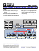
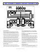
The outputs of PCG A and B can be routed through the DAI
pins and the outputs of PCG C and D can be driven on to the
DAI as well as the DPI pins.
Digital Peripheral Interface (DPI)
The ADSP-2148x SHARC processors have a digital peripheral
interface that provides connections to two serial peripheral
interface ports (SPI), one universal asynchronous receiver-
transmitter (UART), 12 flags, a 2-wire interface (TWI), three
PWM modules (PWM3–1), and two general-purpose timers.
Serial Peripheral (Compatible) Interface (SPI)
The SPI is an industry-standard synchronous serial link,
enabling the SPI-compatible port to communicate with other
SPI compatible devices. The SPI consists of two data pins, one
device select pin, and one clock pin. It is a full-duplex synchro-
nous serial interface, supporting both master and slave modes.
The SPI port can operate in a multimaster environment by
interfacing with up to four other SPI-compatible devices, either
acting as a master or slave device. The SPI-compatible periph-
eral implementation also features programmable baud rate and
clock phase and polarities. The SPI-compatible port uses open
drain drivers to support a multimaster configuration and to
avoid data contention.
UART Port
The processors provide a full-duplex Universal Asynchronous
Receiver/Transmitter (UART) port, which is fully compatible
with PC-standard UARTs. The UART port provides a simpli-
fied UART interface to other peripherals or hosts, supporting
full-duplex, DMA-supported, asynchronous transfers of serial
data. The UART also has multiprocessor communication capa-
bility using 9-bit address detection. This allows it to be used in
multidrop networks through the RS-485 data interface
standard. The UART port also includes support for 5 to 8 data
bits, 1 or 2 stop bits, and none, even, or odd parity. The UART
port supports two modes of operation:
• PIO (programmed I/O)—The processor sends or receives
data by writing or reading I/O-mapped UART registers.
The data is double-buffered on both transmit and receive.
• DMA (direct memory access)—The DMA controller trans-
fers both transmit and receive data. This reduces the
number and frequency of interrupts required to transfer
data to and from memory. The UART has two dedicated
DMA channels, one for transmit and one for receive. These
DMA channels have lower default priority than most DMA
channels because of their relatively low service rates.
Timers
The ADSP-2148x has a total of three timers: a core timer that
can generate periodic software interrupts and two general-
purpose timers that can generate periodic interrupts and be
independently set to operate in one of three modes:
• Pulse waveform generation mode
• Pulse width count/capture mode
• External event watchdog mode
The core timer can be configured to use FLAG3 as a timer
expired signal, and the general-purpose timers have one bidirec-
tional pin and four registers that implement its mode of
operation: a 6-bit configuration register, a 32-bit count register,
a 32-bit period register, and a 32-bit pulse width register. A sin-
gle control and status register enables or disables the general-
purpose timer.
2-Wire Interface Port (TWI)
The TWI is a bidirectional 2-wire, serial bus used to move 8-bit
data while maintaining compliance with the I
2
C bus protocol.
The TWI master incorporates the following features:
• 7-bit addressing
• Simultaneous master and slave operation on multiple
device systems with support for multi master data
arbitration
• Digital filtering and timed event processing
• 100 kbps and 400 kbps data rates
• Low interrupt rate
I/O PROCESSOR FEATURES
The I/O processors provide up to 65 channels of DMA, as well
as an extensive set of peripherals.
DMA Controller
The processor’s on-chip DMA controller allows data transfers
without processor intervention. The DMA controller operates
independently and invisibly to the processor core, allowing
DMA operations to occur while the core is simultaneously exe-
cuting its program instructions. DMA transfers can occur
between the ADSP-2148x’s internal memory and its serial ports,
the SPI-compatible (serial peripheral interface) ports, the IDP
(input data port), the PDAP, or the UART. The DMA channel
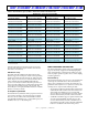
summary is shown in Table 8.
Programs can be downloaded to the ADSP-2148x using DMA
transfers. Other DMA features include interrupt generation
upon completion of DMA transfers and DMA chaining for
automatic linked DMA transfers.
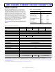
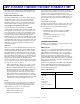
Table 8. DMA Channels
Peripheral DMA Channels
SPORTs 16
IDP/PDAP 8
SPI 2
UART 2
External Port 2
Accelerators 2
Memory-to-Memory 2
MLB
1
1
Automotive models only.
31