
Datasheet

Rev. B | Page 2 of 68 | March 2013
ADSP-21483/ADSP-21486/ADSP-21487/ADSP-21488/ADSP-21489
TABLE OF CONTENTS
Summary ............................................................... 1
General Description ................................................. 3
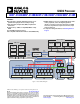
Family Core Architecture ........................................ 4
Family Peripheral Architecture ................................ 7
I/O Processor Features ......................................... 10
System Design .................................................... 11
Development Tools ............................................. 12
Additional Information ........................................ 13
Related Signal Chains .......................................... 13
Pin Function Descriptions ....................................... 14
Specifications ........................................................ 18
Operating Conditions .......................................... 18
Electrical Characteristics ....................................... 19
Absolute Maximum Ratings .................................. 21
ESD Sensitivity ................................................... 21
Maximum Power Dissipation ................................. 21
Package Information ............................................ 21
Timing Specifications ........................................... 22
Output Drive Currents ......................................... 55
Test Conditions .................................................. 55
Capacitive Loading .............................................. 55
Thermal Characteristics ........................................ 56
100-LQFP_EP Lead Assignment ................................ 58
176-Lead LQFP_EP Lead Assignment ......................... 60
Outline Dimensions ................................................ 64
Surface-Mount Design .......................................... 65
Automotive Products .............................................. 66
Ordering Guide ..................................................... 66
REVISION HISTORY
3/13—Revision A to Revision B
Corrected outstanding document errata.
Added section Static Voltage Scaling (SVS) ................... 11
Revised Development Tools ......................................12
Revised MS
0-1
Pin Description in
Pin Function Descriptions ........................................ 14
Revised Electrical Characteristics ................................ 19
Revised Total Power Dissipation .................................20
Added paragraph to SDRAM Interface Timing (166 MHz
SDCLK) ................................................................32
Added footnote 3 to Table 32 in AMI Read ................... 33
Changed Max values in Table 43 in Pulse-Width Modulation
Generators (PWM) ................................................. 45
Added model to Automotive Product Table (Table 63) in
Automotive Products ............................................... 66
Revised Ordering Guide ........................................... 66
Added 450 MHz products and information to the following:
• Tables 1 and 2 in General Description ......................3
• Operating Conditions ........................................18
• Electrical Characteristics ..................................... 19
• Tables 14 and 15 in Total Power Dissipation ........... 20
• Table 20 in Clock Input ......................................24