
Datasheet

Rev. B | Page 4 of 68 | March 2013
ADSP-21483/ADSP-21486/ADSP-21487/ADSP-21488/ADSP-21489
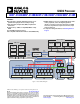
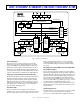
The diagram on Page 1 shows the two clock domains that make
up the ADSP-2148x processors. The core clock domain contains
the following features:
• Two processing elements (PEx, PEy), each of which com-
prises an ALU, multiplier, shifter, and data register file
• Data address generators (DAG1, DAG2)
• Program sequencer with instruction cache
• PM and DM buses capable of supporting 2x64-bit data
transfers between memory and the core at every core pro-
cessor cycle
• One periodic interval timer with pinout
• On-chip SRAM (5 Mbit) and mask-programmable ROM
(4 Mbit)
• JTAG test access port for emulation and boundary scan.
The JTAG provides software debug through user break-
points which allows flexible exception handling.
The block diagram of the ADSP-2148x on Page 1 also shows the
peripheral clock domain (also known as the I/O processor)
which contains the following features:
•IOD0 (peripheral DMA) and IOD1 (external port DMA)
buses for 32-bit data transfers
• Peripheral and external port buses for core connection
• External port with an AMI and SDRAM controller
•4 units for PWM control
• 1 memory-to-memory (MTM) unit for internal-to-internal
memory transfers
• Digital applications interface that includes four precision
clock generators (PCG), an input data port (IDP/PDAP)
for serial and parallel interconnects, an S/PDIF
receiver/transmitter, four asynchronous sample rate con-
verters, eight serial ports, and a flexible signal routing unit
(DAI SRU).
• Digital peripheral interface that includes two timers, a
2-wire interface (TWI), one UART, two serial peripheral
interfaces (SPI), 2 precision clock generators (PCG), pulse
width modulation (PWM), and a flexible signal routing
unit (DPI SRU2).
As shown in the SHARC core block diagram on Page 5, the
processor uses two computational units to deliver a significant
performance increase over the previous SHARC processors on a
range of DSP algorithms. With its SIMD computational hard-
ware, the processors can perform 2.7 GFLOPS running at
450 MHz.
FAMILY CORE ARCHITECTURE
The ADSP-2148x is code compatible at the assembly level with
the ADSP-2147x, ADSP-2146x, ADSP-2137x, ADSP-2136x,
ADSP-2126x, ADSP-21160, and ADSP-21161, and with the first
generation ADSP-2106x SHARC processors. The ADSP-2148x
shares architectural features with the ADSP-2126x, ADSP-
2136x, ADSP-2137x, ADSP-2146x and ADSP-2116x SIMD
SHARC processors, as shown in Figure 2 and detailed in the fol-
lowing sections.
SIMD Computational Engine
The ADSP-2148x contains two computational processing ele-
ments that operate as a single-instruction, multiple-data
(SIMD) engine. The processing elements are referred to as PEX
and PEY and each contains an ALU, multiplier, shifter, and reg-
ister file. PEx is always active, and PEy may be enabled by
setting the PEYEN mode bit in the MODE1 register. SIMD
mode allows the processor to execute the same instruction in
both processing elements, but each processing element operates
on different data. This architecture is efficient at executing math
intensive DSP algorithms.
SIMD mode also affects the way data is transferred between
memory and the processing elements because twice the data
bandwidth is required to sustain computational operation in the
processing elements. Therefore, entering SIMD mode also dou-
bles the bandwidth between memory and the processing
elements. When using the DAGs to transfer data in SIMD
mode, two data values are transferred with each memory or reg-
ister file access.
Independent, Parallel Computation Units
Within each processing element is a set of computational units.
The computational units consist of an arithmetic/logic unit
(ALU), multiplier, and shifter. These units perform all opera-
tions in a single cycle and are arranged in parallel, maximizing
computational throughput. Single multifunction instructions
execute parallel ALU and multiplier operations. In SIMD mode,
the parallel ALU and multiplier operations occur in both pro-
cessing elements. These computation units support IEEE 32-bit
single-precision floating-point, 40-bit extended precision float-
ing-point, and 32-bit fixed-point data formats.
Timer
The processor contains a core timer that can generate periodic
software interrupts. The core timer can be configured to use
FLAG3 as a timer expired signal.
Data Register File
Each processing element contains a general-purpose data regis-
ter file. The register files transfer data between the computation
units and the data buses, and store intermediate results. These
10-port, 32-register (16 primary, 16 secondary) register files,
combined with the processor’s enhanced Harvard architecture,
allow unconstrained data flow between computation units and
internal memory. The registers in PEX are referred to as
R0–R15 and in PEY as S0–S15.
Context Switch
Many of the processor’s registers have secondary registers that
can be activated during interrupt servicing for a fast context
switch. The data registers in the register file, the DAG registers,
and the multiplier result registers all have secondary registers.
The primary registers are active at reset, while the secondary
registers are activated by control bits in a mode control register.