
Datasheet

ADSP-21483/ADSP-21486/ADSP-21487/ADSP-21488/ADSP-21489
Rev. B | Page 5 of 68 | March 2013
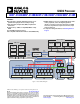
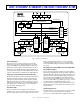
Universal Registers
These registers can be used for general-purpose tasks. The
USTAT (4) registers allow easy bit manipulations (Set, Clear,
Toggle, Test, XOR) for all peripheral registers (control/status).
The data bus exchange register (PX) permits data to be passed
between the 64-bit PM data bus and the 64-bit DM data bus, or
between the 40-bit register file and the PM/DM data bus. These
registers contain hardware to handle the data width difference.
Single-Cycle Fetch of Instruction and Four Operands
The ADSP-2148x features an enhanced Harvard architecture in
which the data memory (DM) bus transfers data and the pro-
gram memory (PM) bus transfers both instructions and data.
With the its separate program and data memory buses and on-
chip instruction cache, the processor can simultaneously fetch
four operands (two over each data bus) and one instruction
(from the cache), all in a single cycle.
Instruction Cache
The processor includes an on-chip instruction cache that
enables three-bus operation for fetching an instruction and four
data values. The cache is selective—only the instructions whose
fetches conflict with PM bus data accesses are cached. This
cache allows full speed execution of core, looped operations
such as digital filter multiply-accumulates, and FFT butterfly
processing.
Data Address Generators With Zero-Overhead Hardware
Circular Buffer Support
The two data address generators (DAGs) are used for indirect
addressing and implementing circular data buffers in hardware.
Circular buffers allow efficient programming of delay lines and
other data structures required in digital signal processing, and
are commonly used in digital filters and Fourier transforms.
The two DAGs contain sufficient registers to allow the creation
of up to 32 circular buffers (16 primary register sets, 16 second-
ary). The DAGs automatically handle address pointer
wraparound, reduce overhead, increase performance, and sim-
plify implementation. Circular buffers can start and end at any
memory location.
Flexible Instruction Set
The 48-bit instruction word accommodates a variety of parallel
operations, for concise programming. For example, the
processor can conditionally execute a multiply, an add, and a
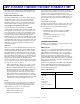
Figure 2. SHARC Core Block Diagram
S
SIMD Core
CACHEINTERRUPT
5 STAGE
PROGRAM SEQUENCER
PM ADDRESS 32
DM ADDRESS 32
DM DATA 64
PM DATA 64
DAG1
16x32
MRF
80-BIT
ALU
MULTIPLIER
SHIFTER
RF
Rx/Fx
PEx
16x40-BIT
JTAG
DMD/PMD 64
PM DATA 48
ASTATx
STYKx
ASTATy
STYKy
TIMER
RF
Sx/SFx
PEy
16x40-BIT
MRB
80-BIT
MSB
80-BIT
MSF
80-BIT
FLAG
SYSTEM
I/F
USTAT
4x32-BIT
PX
64-BIT
DAG2
16x32
MULTIPLIER
DATA
SWAP
PM ADDRESS 24
ALU SHIFTER