
DSP Microcomputers Instructions Manual
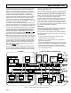
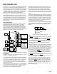
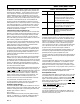

FUNCTIONAL BLOCK DIAGRAM
a
DSP Microcomputers
ADSP-2181/ADSP-2183
FEATURES
PERFORMANCE
30 ns Instruction Cycle Time @ 5.0 Volts
33 MIPS Sustained Performance
34.7 ns Instruction Cycle Time @ 3.3 Volts
Single-Cycle Instruction Execution
Single-Cycle Context Switch
3-Bus Architecture Allows Dual Operand Fetches in
Every Instruction Cycle
Multifunction Instructions
Power-Down Mode Featuring Low CMOS Standby
Power Dissipation with 100 Cycle Recovery from
Power-Down Condition
Low Power Dissipation in Idle Mode
INTEGRATION
ADSP-2100 Family Code Compatible, with Instruction
Set Extensions
80K Bytes of On-Chip RAM, Configured as
16K Words On-Chip Program Memory RAM
16K Words On-Chip Data Memory RAM
Dual Purpose Program Memory for Both Instruction
and Data Storage
Independent ALU, Multiplier/Accumulator, & Barrel
Shifter Computational Units
Two Independent Data Address Generators
Powerful Program Sequencer Provides
Zero Overhead Looping
Conditional Instruction Execution
Programmable 16-Bit Interval Timer with Prescaler
128-Lead TQFP/128-Lead PQFP
SYSTEM INTERFACE
16-Bit Internal DMA Port for High Speed Access to
On-Chip Memory
4 MByte Memory Interface for Storage of Data Tables &
Program Overlays
8-Bit DMA to Byte Memory for Transparent
Program and Data Memory Transfers
I/O Memory Interface with 2048 Locations Supports
Parallel Peripherals
Programmable Memory Strobe & Separate I/O Memory
Space Permits “Glueless” System Design
Programmable Wait State Generation
Two Double-Buffered Serial Ports with Companding
Hardware and Automatic Data Buffering
Automatic Booting of On-Chip Program Memory from
Byte-Wide External Memory, e.g., EPROM, or
Through Internal DMA Port
Six External Interrupts
13 Programmable Flag Pins Provide Flexible System
Signaling
ICE-Port™ Emulator Interface Supports Debugging
in Final Systems
REV. 0
Information furnished by Analog Devices is believed to be accurate and
reliable. However, no responsibility is assumed by Analog Devices for its
use, nor for any infringements of patents or other rights of third parties
which may result from its use. No license is granted by implication or
otherwise under any patent or patent rights of Analog Devices.
ICE-Port is a trademark of Analog Devices, Inc.
© Analog Devices, Inc., 1996
One Technology Way, P.O. Box 9106, Norwood, MA 02062-9106, U.S.A.
Tel: 617/329-4700 Fax: 617/326-8703
GENERAL DESCRIPTION
The ADSP-2181/ADSP-2183 is a single-chip microcomputer
optimized for digital signal processing (DSP) and other high
speed numeric processing applications.
The ADSP-2181/ADSP-2183 combines the ADSP-2100 family
base architecture (three computational units, data address gen-
erators and a program sequencer) with two serial ports, a 16-bit
internal DMA port, a byte DMA port, a programmable timer,
Flag I/O, extensive interrupt capabilities, and on-chip program
and data memory.
The ADSP-2181/ADSP-2183 integrates 80K bytes of on-chip
memory configured as 16K words (24-bit) of program RAM,
and 16K words (16-bit) of data RAM. Power down circuitry is
also provided to meet the low power needs of battery operated
portable equipment. The ADSP-2181 is available in 128-pin
TQFP and 128-pin PQFP packages; the ADSP-2183 is avail-
able in the TQFP package only.
In addition, the ADSP-2181/ADSP-2183 supports new instruc-
tions, which include bit manipulations—bit set, bit clear, bit toggle,
bit test—new ALU constants, new multiplication instruction
(x squared), biased rounding, result free ALU operations, I/O memory
transfers, and global interrupt masking, for increased flexibility.
Fabricated in a high speed, double metal, low power, 0.5 µm
CMOS process, the ADSP-2181 operates with a 30 ns instruc-
tion cycle time (34.7 ns for the ADSP-2183). Every instruction
can execute in a single processor cycle.
The ADSP-2181/ADSP-2183’s flexible architecture and com-
prehensive instruction set allow the processor to perform multiple
operations in parallel. In one processor cycle the ADSP-2181/
ADSP-2183 can:
• generate the next program address
• fetch the next instruction
• perform one or two data moves
• update one or two data address pointers
• perform a computational operation
SERIAL PORTS
MEMORY
FLAGS
PROGRAMMABLE
I/O
BYTE DMA
CONTROLLER
PROGRAM
MEMORY
DATA
MEMORY
EXTERNAL
ADDRESS
BUS
EXTERNAL
DATA
BUS
DMA
BUS
INTERNAL
DMA
PORT
TIMER
SPORT 1SPORT 0
ADSP-2100 BASE
ARCHITECTURE
SHIFTER
MAC
ALU
ARITHMETIC UNITS
POWERDOWN
CONTROL
PROGRAM
SEQUENCER
DAG 0
DAG 1
DATA ADDRESS
GENERATORS
PROGRAM MEMORY ADDRESS
DATA MEMORY ADDRESS
PROGRAM MEMORY DATA
DATA MEMORY DATA