
DSP Microcomputers Instructions Manual


ADSP-2181/ADSP-2183
REV. 0
–5–
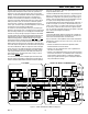
Table I. Interrupt Priority & Interrupt Vector Addresses
Interrupt Vector
Source of Interrupt Address (Hex)
Reset (or Power-Up with PUCR = 1) 0000 (Highest Priority)
Power Down (Nonmaskable) 002C
IRQ2 0004
IRQL1 0008
IRQL0 000C
SPORT0 Transmit 0010
SPORT0 Receive 0014
IRQE 0018
BDMA Interrupt 001C
SPORT1 Transmit or
IRQ1 0020
SPORT1 Receive or
IRQ0 0024
Timer 0028 (Lowest Priority)
Interrupt routines can either be nested with higher priority in-
terrupts taking precedence or processed sequentially. Interrupts
can be masked or unmasked with the IMASK register. Indi-
vidual interrupt requests are logically ANDed with the bits
in IMASK; the highest priority unmasked interrupt is then
selected. The power-down interrupt is nonmaskable.
The ADSP-2181/ADSP-2183 masks all interrupts for one in-
struction cycle following the execution of an instruction that
modifies the IMASK register. This does not affect serial port
autobuffering or DMA transfers.
The interrupt control register, ICNTL, controls interrupt nest-
ing and defines the
IRQ0, IRQ1, and IRQ2 external interrupts
to be either edge- or level-sensitive. The
IRQE pin is an external
edge sensitive interrupt and can be forced and cleared. The
IRQL0 and IRQL1 pins are external level sensitive interrupts.
The IFC register is a write-only register used to force and clear
interrupts.
On-chip stacks preserve the processor status and are automati-
cally maintained during interrupt handling. The stacks are
twelve levels deep to allow interrupt, loop, and subroutine
nesting.
The following instructions allow global enable or disable servic-
ing of the interrupts (including power down), regardless of the
state of IMASK. Disabling the interrupts does not affect serial
port autobuffering or DMA.
ENA INTS;
DIS INTS;
When the processor is reset, interrupt servicing is enabled.
LOW POWER OPERATION
The ADSP-2181/ADSP-2183 has three low power modes that
significantly reduce the power dissipation when the device oper-
ates under standby conditions. These modes are:
• Power Down
• Idle
• Slow Idle
The CLKOUT pin may also be disabled to reduce external
power dissipation.
Power Down
The ADSP-2181/ADSP-2183 processor has a low power
feature that lets the processor enter a very low power dor-
mant state through hardware or software control. Here is a
brief list of power-down features. Refer to the ADSP-2100
Family User’s Manual, Chapter 9 “System Interface” for de-
tailed information about the power-down feature.
• Quick recovery from power down. The processor begins
executing instructions in as few as 100 CLKIN cycles.
• Support for an externally generated TTL or CMOS pro-
cessor clock. The external clock can continue running
during power down without affecting the lowest power rat-
ing and 100 CLKIN cycle recovery.
• Support for crystal operation includes disabling the oscil-
lator to save power (the processor automatically waits 4096
CLKIN cycles for the crystal oscillator to start and stabi-
lize), and letting the oscillator run to allow 100 CLKIN
cycle start up.
• Power down is initiated by either the power-down pin
(
PWD) or the software power-down force bit.
• Interrupt support allows an unlimited number of instruc-
tions to be executed before optionally powering down.
The power-down interrupt also can be used as a non-
maskable, edge sensitive interrupt.
• Context clear/save control allows the processor to con-
tinue where it left off or start with a clean context when
leaving the power-down state.
• The
RESET pin also can be used to terminate power
down.
• Power-down acknowledge pin indicates when the proces-
sor has entered power down.
Processor supply current during power down varies with
temperature, see Figures 8 and 15.
Idle
When the ADSP-2181/ADSP-2183 is in the Idle Mode, the
processor waits indefinitely in a low power state until an
interrupt occurs. When an unmasked interrupt occurs, it is
serviced; execution then continues with the instruction fol-
lowing the IDLE instruction.
Slow Idle
The IDLE instruction is enhanced on the ADSP-2181/
ADSP-2183 to let the processor’s internal clock signal be
slowed, further reducing power consumption. The reduced
clock frequency, a programmable fraction of the normal
clock rate, is specified by a selectable divisor given in the
IDLE instruction. The format of the instruction is
IDLE (n);
where n = 16, 32, 64, or 128. This instruction keeps the
processor fully functional, but operating at the slower clock
rate. While it is in this state, the processor’s other internal
clock signals, such as SCLK, CLKOUT, and timer clock,
are reduced by the same ratio. The default form of the in-
struction, when no clock divisor is given, is the standard
IDLE instruction.