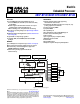
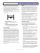
Blackfin Embedded Processor ADSP-BF531/ADSP-BF532/ADSP-BF533 FEATURES PERIPHERALS Up to 600 MHz high performance Blackfin processor Two 16-bit MACs, two 40-bit ALUs, four 8-bit video ALUs, 40-bit shifter RISC-like register and instruction model for ease of programming and compiler-friendly support Advanced debug, trace, and performance monitoring Wide range of operating voltages (see Operating Conditions on Page 20) Qualified for Automotive Applications (see Automotive Products on Page 62) Programmable on
ADSP-BF531/ADSP-BF532/ADSP-BF533 TABLE OF CONTENTS Features ................................................................. 1 Development Tools .............................................. 15 Memory ................................................................ 1 Additional Information ........................................ 16 Peripherals ............................................................. 1 Related Signal Chains ........................................... 16 General Description ....
ADSP-BF531/ADSP-BF532/ADSP-BF533 GENERAL DESCRIPTION The ADSP-BF531/ADSP-BF532/ADSP-BF533 processors are members of the Blackfin® family of products, incorporating the Analog Devices, Inc./Intel Micro Signal Architecture (MSA). Blackfin processors combine a dual-MAC state-of-the-art signal processing engine, the advantages of a clean, orthogonal RISClike microprocessor instruction set, and single instruction, multiple data (SIMD) multimedia capabilities into a single instruction set architecture.
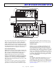
ADSP-BF531/ADSP-BF532/ADSP-BF533 BLACKFIN PROCESSOR CORE As shown in Figure 2 on Page 5, the Blackfin processor core contains two 16-bit multipliers, two 40-bit accumulators, two 40-bit ALUs, four video ALUs, and a 40-bit shifter. The computation units process 8-bit, 16-bit, or 32-bit data from the register file. The compute register file contains eight 32-bit registers. When performing compute operations on 16-bit operand data, the register file operates as 16 independent 16-bit registers.
ADSP-BF531/ADSP-BF532/ADSP-BF533 ADDRESS ARITHMETIC UNIT I3 L3 B3 M3 I2 L2 B2 M2 I1 L1 B1 M1 I0 L0 B0 M0 SP FP P5 DAG1 P4 P3 DAG0 P2 DA1 32 P1 DA0 32 TO MEMORY P0 32 PREG 32 RAB SD 32 LD1 32 LD0 32 ASTAT 32 32 R7.H R6.H R7.L R6.L R5.H R5.L R4.H R4.L R3.H R3.L R2.H R2.L R1.H R1.L R0.H R0.L SEQUENCER ALIGN 16 16 8 8 8 8 DECODE BARREL SHIFTER 40 40 40 A0 32 40 A1 LOOP BUFFER CONTROL UNIT 32 DATA ARITHMETIC UNIT Figure 2.
ADSP-BF531/ADSP-BF532/ADSP-BF533 0xFFFF FFFF 0xFFFF FFFF CORE MMR REGISTERS (2M BYTE) CORE MMR REGISTERS (2M BYTE) 0xFFE0 0000 0xFFE0 0000 SYSTEM MMR REGISTERS (2M BYTE) SYSTEM MMR REGISTERS (2M BYTE) 0xFFC0 0000 0xFFC0 0000 RESERVED RESERVED 0xFFB0 1000 0xFFB0 1000 0xFFB0 0000 0xFFB0 0000 RESERVED RESERVED 0xFFA1 4000 INTERNAL MEMORY MAP 0xFFA1 4000 INSTRUCTION SRAM/CACHE (16K BYTE) 0xFFA1 0000 RESERVED 0xFFA0 C000 INSTRUCTION SRAM (16K BYTE) 0xFFA0 8000 RESERVED 0xFFA0 0000 RESERVED 0xFF90 800
ADSP-BF531/ADSP-BF532/ADSP-BF533 Each event type has an associated register to hold the return address and an associated return-from-event instruction. When an event is triggered, the state of the processor is saved on the supervisor stack. The ADSP-BF531/ADSP-BF532/ADSP-BF533 processors’ event controller consists of two stages, the core event controller (CEC) and the system interrupt controller (SIC).
ADSP-BF531/ADSP-BF532/ADSP-BF533 • CEC interrupt pending register (IPEND) – The IPEND register keeps track of all nested events. A set bit in the IPEND register indicates the event is currently active or nested at some level. This register is updated automatically by the controller but can be read while in supervisor mode. The SIC allows further control of event processing by providing three 32-bit interrupt control and status registers.
ADSP-BF531/ADSP-BF532/ADSP-BF533 The stopwatch function counts down from a programmed value, with one second resolution. When the stopwatch is enabled and the counter underflows, an interrupt is generated. Like other peripherals, the RTC can wake up the processor from sleep mode upon generation of any RTC wakeup event. Additionally, an RTC wakeup event can wake up the processor from deep sleep mode, and wake up the on-chip internal voltage regulator from a powered-down state.
ADSP-BF531/ADSP-BF532/ADSP-BF533 • Interrupts – Each transmit and receive port generates an interrupt upon completing the transfer of a data-word or after transferring an entire data buffer or buffers through DMA. • DMA (direct memory access) – The DMA controller transfers both transmit and receive data. This reduces the number and frequency of interrupts required to transfer data to and from memory. The UART has two dedicated DMA channels, one for transmit and one for receive.
ADSP-BF531/ADSP-BF532/ADSP-BF533 PFx pins defined as inputs can be configured to generate hardware interrupts, while output PFx pins can be triggered by software interrupts. • GPIO interrupt sensitivity registers – The two GPIO interrupt sensitivity registers specify whether individual PFx pins are level- or edge-sensitive and specify—if edge-sensitive—whether just the rising edge or both the rising and falling edges of the signal are significant.
ADSP-BF531/ADSP-BF532/ADSP-BF533 Active Operating Mode—Moderate Power Savings In the active mode, the PLL is enabled but bypassed. Because the PLL is bypassed, the processor’s core clock (CCLK) and system clock (SCLK) run at the input clock (CLKIN) frequency. DMA access is available to appropriately configured L1 memories. In the active mode, it is possible to disable the PLL through the PLL control register (PLL_CTL).
ADSP-BF531/ADSP-BF532/ADSP-BF533 For further details on the on-chip voltage regulator and related board design guidelines, see the Switching Regulator Design Considerations for ADSP-BF533 Blackfin Processors (EE-228) applications note on the Analog Devices web site (www.analog.com)—use site search on “EE-228”.
ADSP-BF531/ADSP-BF532/ADSP-BF533 As shown in Figure 9, the core clock (CCLK) and system peripheral clock (SCLK) are derived from the input clock (CLKIN) signal. An on-chip PLL is capable of multiplying the CLKIN signal by a user programmable 0.5 to 64 multiplication factor (bounded by specified minimum and maximum VCO frequencies). The default multiplier is 10, but it can be modified by a software instruction sequence.
ADSP-BF531/ADSP-BF532/ADSP-BF533 more bytes until the flag is deasserted. The GPIO pin is chosen by the user and this information is transferred to the Blackfin processor via bits[10:5] of the FLAG header in the LDR image. For each of the boot modes, a 10-byte header is first read from an external memory device. The header specifies the number of bytes to be transferred and the memory destination address. Multiple memory blocks can be loaded by any boot sequence.
ADSP-BF531/ADSP-BF532/ADSP-BF533 Board Support Packages for Evaluation Hardware ADDITIONAL INFORMATION Software support for the EZ-KIT Lite evaluation boards and EZExtender daughter cards is provided by software add-ins called Board Support Packages (BSPs). The BSPs contain the required drivers, pertinent release notes, and select example code for the given evaluation hardware. A download link for a specific BSP is located on the web page for the associated EZ-KIT or EZExtender product.
ADSP-BF531/ADSP-BF532/ADSP-BF533 PIN DESCRIPTIONS The ADSP-BF531/ADSP-BF532/ADSP-BF533 processors pin definitions are listed in Table 9. All pins are three-stated during and immediately after reset, except the memory interface, asynchronous memory control, and synchronous memory control pins. These pins are all driven high, with the exception of CLKOUT, which toggles at the system clock rate. During hibernate, all outputs are threestated unless otherwise noted in Table 9.
ADSP-BF531/ADSP-BF532/ADSP-BF533 Table 9.
ADSP-BF531/ADSP-BF532/ADSP-BF533 Table 9.
ADSP-BF531/ADSP-BF532/ADSP-BF533 SPECIFICATIONS Component specifications are subject to change without notice.
ADSP-BF531/ADSP-BF532/ADSP-BF533 The following three tables describe the voltage/frequency requirements for the processor clocks. Take care in selecting MSEL, SSEL, and CSEL ratios so as not to exceed the maximum core clock (Table 10 and Table 11) and system clock (Table 13) specifications. Table 12 describes phase-locked loop operating conditions. Table 10. Core Clock (CCLK) Requirements—500 MHz, 533 MHz, and 600 MHz Models Parameter fCCLK CCLK Frequency (VDDINT = 1.
ADSP-BF531/ADSP-BF532/ADSP-BF533 ELECTRICAL CHARACTERISTICS 400 MHz1 Parameter Test Conditions Min Typical 500 MHz/533 MHz/600 MHz2 Max Min Typical Max Unit VOH High Level VDDEXT = 1.75 V, IOH = –0.5 mA Output Voltage3 VDDEXT = 2.25 V, IOH = –0.5 mA VDDEXT = 3.0 V, IOH = –0.5 mA VOL Low Level VDDEXT = 1.75 V, IOL = 2.0 mA Output Voltage3 VDDEXT = 2.25 V/3.0 V, IOL = 2.0 mA 0.2 0.4 0.2 0.4 V V IIH High Level Input VDDEXT = Max, VIN = VDD Max Current4 10.0 10.
ADSP-BF531/ADSP-BF532/ADSP-BF533 5 Applies to JTAG input pins (TCK, TDI, TMS, TRST). Absolute value. 7 Applies to three-statable pins. 8 Applies to all signal pins. 9 Guaranteed, but not tested. 10 See the ADSP-BF533 Blackfin Processor Hardware Reference Manual for definitions of sleep, deep sleep, and hibernate operating modes. 11 See Table 16 for the list of IDDINT power vectors covered by various Activity Scaling Factors (ASF).
ADSP-BF531/ADSP-BF532/ADSP-BF533 Table 16. Activity Scaling Factors IDDINT Power Vector1 IDD-PEAK IDD-HIGH IDD-TYP IDD-APP IDD-NOP IDD-IDLE 1 2 Activity Scaling Factor (ASF)2 1.27 1.25 1.00 0.86 0.72 0.41 See EE-229 for power vector definitions. All ASF values determined using a 10:1 CCLK:SCLK ratio. Table 17. Dynamic Current (mA, with ASF = 1.0)1 Voltage (VDDINT)2 Frequency (MHz)2 50 100 200 250 300 375 400 425 475 500 533 600 1 2 0.80 V 12.7 22.6 40.8 50.1 N/A N/A N/A N/A N/A N/A N/A N/A 0.85 V 13.
ADSP-BF531/ADSP-BF532/ADSP-BF533 ABSOLUTE MAXIMUM RATINGS Stresses greater than those listed in Table 18 may cause permanent damage to the device. These are stress ratings only. Functional operation of the device at these or any other conditions greater than those indicated in the operational sections of this specification is not implied. Exposure to absolute maximum rating conditions for extended periods can affect device reliability. Table 18.
ADSP-BF531/ADSP-BF532/ADSP-BF533 PACKAGE INFORMATION The information presented in Figure 10 and Table 20 provides details about the package branding for the Blackfin processors. For a complete listing of product availability, see the Ordering Guide on Page 63. a ADSP-BF53x tppZccc vvvvvv.x n.n #yyww country_of_origin B Figure 10. Product Information on Package Table 20.
ADSP-BF531/ADSP-BF532/ADSP-BF533 TIMING SPECIFICATIONS Clock and Reset Timing Table 21 and Figure 11 describe clock and reset operations. Per Absolute Maximum Ratings on Page 25, combinations of CLKIN and clock multipliers/divisors must not result in core/ system clocks exceeding the maximum limits allowed for the processor, including system clock restrictions related to supply voltage. Table 21.
ADSP-BF531/ADSP-BF532/ADSP-BF533 Asynchronous Memory Read Cycle Timing Table 23. Asynchronous Memory Read Cycle Timing Parameter Timing Requirements tSDAT DATA15–0 Setup Before CLKOUT tHDAT DATA15–0 Hold After CLKOUT tSARDY ARDY Setup Before CLKOUT tHARDY ARDY Hold After CLKOUT Switching Characteristics Output Delay After CLKOUT1 tDO tHO Output Hold After CLKOUT 1 1 VDDEXT = 1.8 V Min Max VDDEXT = 2.5 V/3.3 V Min Max Unit 2.1 1.0 4.0 1.0 2.1 0.8 4.0 0.0 6.0 6.0 1.0 0.
ADSP-BF531/ADSP-BF532/ADSP-BF533 Asynchronous Memory Write Cycle Timing Table 24. Asynchronous Memory Write Cycle Timing Parameter Timing Requirements tSARDY ARDY Setup Before CLKOUT tHARDY ARDY Hold After CLKOUT Switching Characteristics tDDAT DATA15–0 Disable After CLKOUT tENDAT DATA15–0 Enable After CLKOUT Output Delay After CLKOUT1 tDO tHO Output Hold After CLKOUT 1 1 VDDEXT = 1.8 V Min Max VDDEXT = 2.5 V/3.3 V Min Max Unit 4.0 1.0 4.0 0.0 6.0 1.0 6.0 1.0 6.0 1.
ADSP-BF531/ADSP-BF532/ADSP-BF533 SDRAM Interface Timing Table 25. SDRAM Interface Timing1 Parameter Timing Requirements tSSDAT DATA Setup Before CLKOUT tHSDAT DATA Hold After CLKOUT Switching Characteristics tDCAD Command, ADDR, Data Delay After CLKOUT2 tHCAD Command, ADDR, Data Hold After CLKOUT2 Data Disable After CLKOUT tDSDAT tENSDAT Data Enable After CLKOUT tSCLK CLKOUT Period3 tSCLKH CLKOUT Width High tSCLKL CLKOUT Width Low VDDEXT = 1.8 V Min Max VDDEXT = 2.5 V/3.3 V Min Max Unit 2.1 0.8 1.5 0.
ADSP-BF531/ADSP-BF532/ADSP-BF533 External Port Bus Request and Grant Cycle Timing Table 26 and Figure 16 describe external port bus request and bus grant operations. Table 26.
ADSP-BF531/ADSP-BF532/ADSP-BF533 Parallel Peripheral Interface Timing Table 27 and Figure 17 through Figure 22 describe parallel peripheral interface operations. Table 27.
ADSP-BF531/ADSP-BF532/ADSP-BF533 DATA SAMPLED FRAME SYNC SAMPLED PPI_CLK tSFSPE tPCLKW tHFSPE tPCLK PPI_FS1/2 tSDRPE tHDRPE PPI_DATA Figure 19. PPI GP Rx Mode with External Frame Sync Timing (PPI_CONTROL Bit 8 = 0) FRAME SYNC DRIVEN DATA DRIVEN DATA DRIVEN tPCLK PPI_CLK tHOFSPE tDFSPE tPCLKW PPI_FS1/2 tDDTPE tHDTPE PPI_DATA Figure 20.
ADSP-BF531/ADSP-BF532/ADSP-BF533 Serial Port Timing Table 28 through Table 31 on Page 37 and Figure 23 on Page 35 through Figure 26 on Page 37 describe Serial Port operations. Table 28.
ADSP-BF531/ADSP-BF532/ADSP-BF533 DATA RECEIVE—INTERNAL CLOCK DATA RECEIVE—EXTERNAL CLOCK DRIVE EDGE DRIVE EDGE SAMPLE EDGE SAMPLE EDGE tSCLKE tSCLKEW tSCLKIW RSCLKx RSCLKx tDFSE tDFSI tHOFSI tHOFSE RFSx (OUTPUT) RFSx (OUTPUT) tSFSI tHFSI RFSx (INPUT) tSFSE tHFSE tSDRE tHDRE RFSx (INPUT) tSDRI tHDRI DRx DRx DATA TRANSMIT—INTERNAL CLOCK DRIVE EDGE DATA TRANSMIT—EXTERNAL CLOCK SAMPLE EDGE DRIVE EDGE tSCLKIW SAMPLE EDGE t SCLKEW TSCLKx tSCLKE TSCLKx tD FSI tDFSE tHOFSI tHOF
ADSP-BF531/ADSP-BF532/ADSP-BF533 Table 30. Serial Ports—Enable and Three-State Parameter Switching Characteristics tDTENE Data Enable Delay from External TSCLKx1 tDDTTE Data Disable Delay from External TSCLKx1, 2, 3 tDTENI Data Enable Delay from Internal TSCLKx1 tDDTTI Data Disable Delay from Internal TSCLKx1, 2, 3 Min VDDEXT = 1.8 V Max 0 VDDEXT = 2.5 V/3.3 V Min Max Unit 0 10.0 2.0 2.0 3.0 1 Referenced to drive edge. Applicable to multichannel mode only. 3 TSCLKx is tied to RSCLKx.
ADSP-BF531/ADSP-BF532/ADSP-BF533 Table 31. External Late Frame Sync VDDEXT = 1.8 V VDDEXT = 1.8 V LQFP/PBGA Packages CSP_BGA Package Min Max Min Max Parameter Switching Characteristics tDDTLFSE Data Delay from Late External TFSx or External RFSx in multichannel mode with MCMEN = 01, 2 tDTENLFS Data Enable from Late FS or in multichannel mode 0 with MCMEN = 01, 2 1 2 10.5 10.0 0 In multichannel mode, TFSx enable and TFSx valid follow tDTENLFS and tDDTLFSE.
ADSP-BF531/ADSP-BF532/ADSP-BF533 Serial Peripheral Interface (SPI) Port—Master Timing Table 32. Serial Peripheral Interface (SPI) Port—Master Timing VDDEXT = 1.8 V VDDEXT = 1.8 V LQFP/PBGA Packages CSP_BGA Package Min Max Min Max Parameter Timing Requirements tSSPIDM Data Input Valid to SCK Edge (Data Input Setup) 10.5 –1.5 tHSPIDM SCK Sampling Edge to Data Input Invalid Switching Characteristics tSDSCIM SPISELx Low to First SCK Edge 2 × tSCLK – 1.5 tSPICHM Serial Clock High Period 2 × tSCLK – 1.
ADSP-BF531/ADSP-BF532/ADSP-BF533 Serial Peripheral Interface (SPI) Port—Slave Timing Table 33. Serial Peripheral Interface (SPI) Port—Slave Timing VDDEXT = 1.8 V VDDEXT = 1.8 V LQFP/PBGA Packages CSP_BGA Package Min Max Min Max Parameter Timing Requirements tSPICHS Serial Clock High Period 2 × tSCLK –1.5 2 × tSCLK –1.5 tSPICLS Serial Clock Low Period tSPICLK Serial Clock Period 4 × tSCLK tHDS Last SCK Edge to SPISS Not Asserted 2 × tSCLK –1.5 tSPITDS Sequential Transfer Delay 2 × tSCLK –1.
ADSP-BF531/ADSP-BF532/ADSP-BF533 General-Purpose I/O Port F Pin Cycle Timing Table 34. General-Purpose I/O Port F Pin Cycle Timing Parameter Timing Requirement tWFI GPIO Input Pulse Width Switching Characteristic tGPOD GPIO Output Delay from CLKOUT Low VDDEXT = 1.8 V Min Max VDDEXT = 2.5 V/3.3 V Min Max Unit tSCLK + 1 tSCLK + 1 6 CLKOUT tGPOD GPIO OUTPUT tWFI GPIO INPUT Figure 29.
ADSP-BF531/ADSP-BF532/ADSP-BF533 Timer Clock Timing Table 35 and Figure 30 describe timer clock timing. Table 35. Timer Clock Timing Parameter Switching Characteristic tTODP Timer Output Update Delay After PPI_CLK High Min Max Unit 12 ns PPI_CLK tTODP TMRx OUTPUT Figure 30. Timer Clock Timing Timer Cycle Timing Table 36 and Figure 31 describe timer expired operations.
ADSP-BF531/ADSP-BF532/ADSP-BF533 JTAG Test and Emulation Port Timing Table 37. JTAG Port Timing Parameter Timing Requirements tTCK TCK Period tSTAP TDI, TMS Setup Before TCK High tHTAP TDI, TMS Hold After TCK High tSSYS System Inputs Setup Before TCK High1 tHSYS System Inputs Hold After TCK High1 tTRSTW TRST Pulse Width2 (Measured in TCK Cycles) Switching Characteristics tDTDO TDO Delay from TCK Low tDSYS System Outputs Delay After TCK Low3 Min VDDEXT = 1.8 V Max 20 4 4 4 5 4 0 1 10 12 VDDEXT = 2.
ADSP-BF531/ADSP-BF532/ADSP-BF533 OUTPUT DRIVE CURRENTS 150 150 VDDEXT = 2.75V VDDEXT = 2.50V VDDEXT = 2.25V SOURCE CURRENT (mA) 100 VDDEXT = 2.75V VDDEXT = 2.50V VDDEXT = 2.25V 100 SOURCE CURRENT (mA) Figure 33 through Figure 44 show typical current-voltage characteristics for the output drivers of the processors. The curves represent the current drive capability of the output drivers as a function of output voltage. 50 50 0 VOH –50 –100 0 –150 VOH VOL 0 0.5 1.0 1.5 2.0 2.5 3.
ADSP-BF531/ADSP-BF532/ADSP-BF533 60 100 40 SOURCE CURRENT (mA) VDDEXT = 2.75V VDDEXT = 2.50V VDDEXT = 2.25V SOURCE CURRENT (mA) 20 0 VOH –20 –40 80 VDDEXT = 2.75V VDDEXT = 2.50V 60 VDDEXT = 2.25V 40 20 0 VOH –20 –40 –60 VOL VOL –80 –60 0 0.5 1.0 1.5 2.0 2.5 3.0 –100 SOURCE VOLTAGE (V) 0 0.5 1.0 1.5 2.0 2.5 3.0 SOURCE VOLTAGE (V) Figure 39. Drive Current C (VDDEXT = 2.5 V) Figure 42. Drive Current D (VDDEXT = 2.5 V) 30 VDDEXT = 1.9V VDDEXT = 1.8V 60 VDDEXT = 1.
ADSP-BF531/ADSP-BF532/ADSP-BF533 TEST CONDITIONS All timing parameters appearing in this data sheet were measured under the conditions described in this section. Figure 45 shows the measurement point for ac measurements (except output enable/disable). The measurement point VMEAS is 0.95 V for VDDEXT (nominal) = 1.8 V or 1.5 V for VDDEXT (nominal) = 2.5 V/ 3.3 V. The time tDECAY is calculated with test loads CL and IL, and with V equal to 0.1 V for VDDEXT (nominal) = 1.8 V or 0.
ADSP-BF531/ADSP-BF532/ADSP-BF533 Capacitive Loading 16 Output delays and holds are based on standard capacitive loads: 30 pF on all pins (see Figure 47). VLOAD is 0.95 V for VDDEXT (nominal) = 1.8 V or 1.5 V for VDDEXT (nominal) = 2.5 V/3.3 V. Figure 48 through Figure 59 on Page 48 show how output rise time varies with capacitance. The delay and hold specifications given should be derated by a factor derived from these figures. The graphs in these figures may not be linear outside the ranges shown.
ADSP-BF531/ADSP-BF532/ADSP-BF533 30 12 RISE AND FALL TIME ns (10% to 90%) RISE AND FALL TIME ns (10% to 90%) 14 RISE TIME 10 8 FALL TIME 6 4 25 RISE TIME 20 FALL TIME 15 10 5 2 0 0 0 50 100 150 LOAD CAPACITANCE (pF) 200 0 250 Figure 51. Typical Rise and Fall Times (10% to 90%) vs. Load Capacitance for Driver B at VDDEXT = 1.75 V 50 100 150 LOAD CAPACITANCE (pF) 200 250 Figure 54. Typical Rise and Fall Times (10% to 90%) vs. Load Capacitance for Driver C at VDDEXT = 1.
ADSP-BF531/ADSP-BF532/ADSP-BF533 SCK (66MHz DRIVER), VDDEXT = 1.7V RISE AND FALL TIME ns (10% to 90%) 18 16 RISE TIME 14 12 FALL TIME 10 8 6 4 2 0 0 50 100 150 200 250 LOAD CAPACITANCE (pF) Figure 57. Typical Rise and Fall Times (10% to 90%) vs. Load Capacitance for Driver D at VDDEXT = 1.75 V RISE AND FALL TIME ns (10% to 90%) 18 16 14 RISE TIME 12 10 FALL TIME 8 6 4 2 0 0 50 100 150 LOAD CAPACITANCE (pF) 200 250 Figure 58. Typical Rise and Fall Times (10% to 90%) vs.
ADSP-BF531/ADSP-BF532/ADSP-BF533 THERMAL CHARACTERISTICS Table 38. Thermal Characteristics for BC-160 Package To determine the junction temperature on the application printed circuit board, use: T J = T CASE + JT P D Parameter Condition Typical Unit JA 0 Linear m/s Airflow 27.1 JMA 1 Linear m/s Airflow 23.85 JMA 2 Linear m/s Airflow 22.7 JC Not Applicable 7.26 JT 0 Linear m/s Airflow 0.14 JT 1 Linear m/s Airflow 0.26 JT 2 Linear m/s Airflow 0.
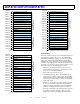
ADSP-BF531/ADSP-BF532/ADSP-BF533 160-BALL CSP_BGA BALL ASSIGNMENT Table 41 lists the CSP_BGA ball assignment by signal. Table 42 on Page 51 lists the CSP_BGA ball assignment by ball number. Table 41. 160-Ball CSP_BGA Ball Assignment (Alphabetical by Signal) Signal ABE0 ABE1 ADDR1 ADDR2 ADDR3 ADDR4 ADDR5 ADDR6 ADDR7 ADDR8 ADDR9 ADDR10 ADDR11 ADDR12 ADDR13 ADDR14 ADDR15 ADDR16 ADDR17 ADDR18 ADDR19 AMS0 AMS1 AMS2 AMS3 AOE ARDY ARE AWE BG BGH BMODE0 BMODE1 BR CLKIN CLKOUT DATA0 DATA1 DATA2 DATA3 Ball No.
ADSP-BF531/ADSP-BF532/ADSP-BF533 Table 42. 160-Ball CSP_BGA Ball Assignment (Numerical by Ball Number) Ball No. A1 A2 A3 A4 A5 A6 A7 A8 A9 A10 A11 A12 A13 A14 B1 B2 B3 B4 B5 B6 B7 B8 B9 B10 B11 B12 B13 B14 C1 C2 C3 C4 C5 C6 C7 C8 C9 C10 C11 C12 Signal VDDEXT PF8 PF9 PF10 PF11 PF14 PPI2 RTXO RTXI GND XTAL CLKIN VROUT0 GND PF4 PF5 PF6 PF7 PF12 PF13 PPI3 PPI1 VDDRTC NMI GND VROUT1 SCKE CLKOUT PF1 PF2 PF3 GND GND PF15 VDDEXT PPI0 PPI_CLK RESET GND VDDEXT Ball No.
ADSP-BF531/ADSP-BF532/ADSP-BF533 Figure 60 shows the top view of the CSP_BGA ball configuration. Figure 61 shows the bottom view of the CSP_BGA ball configuration. 1 2 3 4 5 6 7 8 9 14 13 12 11 10 9 10 11 12 13 14 8 7 6 5 4 3 2 1 A A B B C C D D E E F F G G H H J J K K L L M M N N P P KEY: KEY: VDDINT VDDEXT GND VDDRTC VDDINT GND VDDRTC I/O VROUT VDDEXT I/O VROUT Figure 61. 160-Ball CSP_BGA Ground Configuration (Bottom View) Figure 60.
ADSP-BF531/ADSP-BF532/ADSP-BF533 169-BALL PBGA BALL ASSIGNMENT Table 43 lists the PBGA ball assignment by signal. Table 44 on Page 54 lists the PBGA ball assignment by ball number. Table 43. 169-Ball PBGA Ball Assignment (Alphabetical by Signal) Signal ABE0 ABE1 ADDR1 ADDR2 ADDR3 ADDR4 ADDR5 ADDR6 ADDR7 ADDR8 ADDR9 ADDR10 ADDR11 ADDR12 ADDR13 ADDR14 ADDR15 ADDR16 ADDR17 ADDR18 ADDR19 AMS0 AMS1 AMS2 AMS3 AOE ARDY ARE AWE BG BGH BMODE0 BMODE1 BR CLKIN CLKOUT DATA0 DATA1 DATA2 DATA3 Ball No.
ADSP-BF531/ADSP-BF532/ADSP-BF533 Table 44. 169-Ball PBGA Ball Assignment (Numerical by Ball Number) Ball No. A1 A2 A3 A4 A5 A6 A7 A8 A9 A10 A11 A12 A13 A14 A15 A16 A17 B1 B2 B3 B4 B5 B6 B7 B8 B9 B10 B11 B12 B13 B14 B15 B16 B17 C1 C2 C16 C17 D1 D2 Signal PF4 PF5 PF7 PF9 PF11 PF12 PF14 PPI3 PPI1 RTXI RTXO RESET XTAL CLKIN SRAS SCAS SMS PF2 VDDEXT PF6 PF8 PF10 PF13 PF15 PPI2 PPI0 PPI_CLK NMI VROUT0 VROUT1 SCKE SA10 GND SWE PF1 PF3 ARDY BR SCK PF0 Ball No.
ADSP-BF531/ADSP-BF532/ADSP-BF533 A1 BALL PAD CORNER A B C D E F KEY G H V GND NC V I/O V ROUT DDINT J K DDEXT L M N P R T U 2 1 4 6 8 5 3 10 7 12 11 9 14 16 15 13 17 TOP VIEW Figure 62. 169-Ball PBGA Ground Configuration (Top View) A1 BALL PAD CORNER A B KEY: C D E V DDINT GND NC V DDEXT I/O V F G H J K L M N P R T U 17 16 15 14 13 12 11 10 9 8 7 6 5 4 3 2 1 BOTTOM VIEW Figure 63. 169-Ball PBGA Ground Configuration (Bottom View) Rev.
ADSP-BF531/ADSP-BF532/ADSP-BF533 176-LEAD LQFP PINOUT Table 45 lists the LQFP pinout by signal. Table 46 on Page 57 lists the LQFP pinout by lead number. Table 45. 176-Lead LQFP Pin Assignment (Alphabetical by Signal) Signal ABE0 ABE1 ADDR1 ADDR2 ADDR3 ADDR4 ADDR5 ADDR6 ADDR7 ADDR8 ADDR9 ADDR10 ADDR11 ADDR12 ADDR13 ADDR14 ADDR15 ADDR16 ADDR17 ADDR18 ADDR19 AMS0 AMS1 AMS2 AMS3 AOE ARDY ARE AWE BG BGH BMODE0 BMODE1 BR CLKIN CLKOUT DATA0 DATA1 DATA2 Lead No.
ADSP-BF531/ADSP-BF532/ADSP-BF533 Table 46. 176-Lead LQFP Pin Assignment (Numerical by Lead Number) Lead No. 1 2 3 4 5 6 7 8 9 10 11 12 13 14 15 16 17 18 19 20 21 22 23 24 25 26 27 28 29 30 31 32 33 34 35 36 37 38 39 40 Signal GND GND GND VROUT1 VROUT0 VDDEXT GND GND GND CLKIN XTAL VDDEXT RESET NMI GND RTXO RTXI VDDRTC GND VDDEXT PPI_CLK PPI0 PPI1 PPI2 VDDINT PPI3 PF15 PF14 PF13 GND VDDEXT PF12 PF11 PF10 PF9 PF8 PF7 PF6 GND GND Lead No.
ADSP-BF531/ADSP-BF532/ADSP-BF533 OUTLINE DIMENSIONS Dimensions in the outline dimension figures are shown in millimeters. 0.75 0.60 0.45 26.20 26.00 SQ 25.80 1.60 MAX 133 132 176 1 PIN 1 24.20 24.00 SQ 23.80 TOP VIEW (PINS DOWN) 1.45 1.40 1.35 0.15 0.05 SEATING PLANE 0.20 0.09 7° 3.5° 0° 0.08 MAX COPLANARITY 89 44 45 VIEW A VIEW A ROTATED 90° CCW 88 0.50 BSC LEAD PITCH COMPLIANT TO JEDEC STANDARDS MS-026-BGA Figure 64.
ADSP-BF531/ADSP-BF532/ADSP-BF533 A1 BALL CORNER 12.10 12.00 SQ 11.90 A B C D E F G H J K L M N P 10.40 BSC SQ 0.80 BSC TOP VIEW 1.70 1.60 1.35 A1 BALL CORNER 14 13 12 11 10 9 8 7 6 5 4 3 2 1 BOTTOM VIEW DETAIL A DETAIL A 1.31 1.21 1.11 0.40 NOM 0.25 MIN SEATING PLANE *0.55 COPLANARITY 0.45 0.12 0.40 BALL DIAMETER *COMPLIANT TO JEDEC STANDARDS MO-205-AE WITH THE EXCEPTION TO BALL DIAMETER. Figure 65.
ADSP-BF531/ADSP-BF532/ADSP-BF533 A1 CORNER INDEX AREA 19.20 19.00 SQ 18.80 17 A1 BALL PAD INDICATOR 17.05 16.95 SQ 16.85 TOP VIEW 16 15 14 12 10 8 6 4 2 13 11 9 7 5 3 1 A B C D E F G H J K L M N P R T U 16.00 BSC SQ 1.00 BSC BOTTOM VIEW 2.50 2.23 1.97 DETAIL A 0.65 0.56 0.45 0.50 NOM 0.40 MIN SEATING PLANE DETAIL A 0.70 0.60 0.50 BALL DIAMETER COMPLIANT TO JEDEC STANDARDS MS-034-AAG-2 Figure 66. 169-Ball Plastic Ball Grid Array [PBGA] (B-169) Dimensions shown in millimeters Rev.
ADSP-BF531/ADSP-BF532/ADSP-BF533 SURFACE-MOUNT DESIGN Table 47 is provided as an aid to PCB design. For industrystandard design recommendations, refer to IPC-7351, Generic Requirements for Surface-Mount Design and Land Pattern Standard. Table 47. BGA Data for Use with Surface-Mount Design Package Chip Scale Package Ball Grid Array (CSP_BGA) BC-160-2 Plastic Ball Grid Array (PBGA) B-169 Rev. I Ball Attach Type Solder Mask Defined Solder Mask Defined | Page 61 of 64 | August 2013 Solder Mask Opening 0.
ADSP-BF531/ADSP-BF532/ADSP-BF533 AUTOMOTIVE PRODUCTS The ADBF531W, ADBF532W, and ADBF533W models are available with controlled manufacturing to support the quality and reliability requirements of automotive applications. Note that these automotive models may have specifications that differ from the commercial models and designers should review the Specifications section of this data sheet carefully. Only the auto- motive grade products shown in Table 48 are available for use in automotive applications.
ADSP-BF531/ADSP-BF532/ADSP-BF533 ORDERING GUIDE Model 1 Temperature Range2 Speed Grade (Max) Package Description Package Option ADSP-BF531SBB400 –40°C to +85°C 400 MHz 169-Ball PBGA B-169 ADSP-BF531SBBZ400 –40°C to +85°C 400 MHz 169-Ball PBGA B-169 ADSP-BF531SBBC400 –40°C to +85°C 400 MHz 160-Ball CSP_BGA BC-160-2 ADSP-BF531SBBCZ400 –40°C to +85°C 400 MHz 160-Ball CSP_BGA BC-160-2 ADSP-BF531SBBCZ4RL –40°C to +85°C 400 MHz 160-Ball CSP_BGA, 13" Tape and Reel BC-160-2 ADSP-BF531
ADSP-BF531/ADSP-BF532/ADSP-BF533 ©2013 Analog Devices, Inc. All rights reserved. Trademarks and registered trademarks are the property of their respective owners. D03728-0-8/13(I) Rev.