
Datasheet

Rev. I | Page 2 of 64 | August 2013
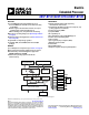
ADSP-BF531/ADSP-BF532/ADSP-BF533
TABLE OF CONTENTS
Features ................................................................. 1
Memory ................................................................ 1
Peripherals ............................................................. 1
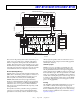
General Description ................................................. 3
Portable Low Power Architecture ............................. 3
System Integration ................................................ 3
Processor Peripherals ............................................. 3
Blackfin Processor Core .......................................... 4
Memory Architecture ............................................ 4
DMA Controllers .................................................. 8
Real-Time Clock ................................................... 8
Watchdog Timer .................................................. 9
Timers ............................................................... 9
Serial Ports (SPORTs) ............................................ 9
Serial Peripheral Interface (SPI) Port ....................... 10
UART Port ........................................................ 10
General-Purpose I/O Port F ................................... 10
Parallel Peripheral Interface ................................... 11
Dynamic Power Management ................................ 11
Voltage Regulation .............................................. 13
Clock Signals ..................................................... 13
Booting Modes ................................................... 14
Instruction Set Description ................................... 15
Development Tools .............................................. 15
Additional Information ........................................ 16
Related Signal Chains ........................................... 16
Pin Descriptions .................................................... 17
Specifications ........................................................ 20
Operating Conditions ........................................... 20
Electrical Characteristics ....................................... 22
Absolute Maximum Ratings ................................... 25
ESD Sensitivity ................................................... 25
Package Information ............................................ 26
Timing Specifications ........................................... 27
Output Drive Currents ......................................... 43
Test Conditions .................................................. 45
Thermal Characteristics ........................................ 49
160-Ball CSP_BGA Ball Assignment ........................... 50
169-Ball PBGA Ball Assignment ................................. 53
176-Lead LQFP Pinout ............................................ 56
Outline Dimensions ................................................ 58
Surface-Mount Design .......................................... 61
Automotive Products .............................................. 62
Ordering Guide ..................................................... 63
REVISION HISTORY
8/13— Rev. H to Rev. I
Updated Development Tools .................................... 15
Corrected Conditions value of the V
IL
specification in
Operating Conditions ............................................. 20
Added notes to Table 30 in
Serial Ports—Enable and Three-State .......................... 36
Added Timer Clock Timing ...................................... 41
Revised Timer Cycle Timing ..................................... 41
Updated Ordering Guide ......................................... 63