
Datasheet

Rev. I | Page 6 of 64 | August 2013
ADSP-BF531/ADSP-BF532/ADSP-BF533
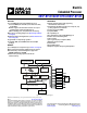
Event Handling
The event controller on the processors handle all asynchronous
and synchronous events to the processor. The ADSP-BF531/
ADSP-BF532/ADSP-BF533 processors provide event handling
that supports both nesting and prioritization. Nesting allows
multiple event service routines to be active simultaneously. Pri-
oritization ensures that servicing of a higher priority event takes
precedence over servicing of a lower priority event. The control-
ler provides support for five different types of events:
• Emulation – An emulation event causes the processor to
enter emulation mode, allowing command and control of
the processor via the JTAG interface.
• Reset – This event resets the processor.
• Nonmaskable Interrupt (NMI) – The NMI event can be
generated by the software watchdog timer or by the NMI
input signal to the processor. The NMI event is frequently
used as a power-down indicator to initiate an orderly shut-
down of the system.
• Exceptions – Events that occur synchronously to program
flow (i.e., the exception is taken before the instruction is
allowed to complete). Conditions such as data alignment
violations and undefined instructions cause exceptions.
• Interrupts – Events that occur asynchronously to program
flow. They are caused by input pins, timers, and other
peripherals, as well as by an explicit software instruction.
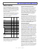
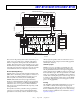
Figure 3. ADSP-BF531 Internal/External Memory Map
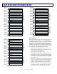
Figure 4. ADSP-BF532 Internal/External Memory Map
CORE MMR REGISTERS (2M BYTE)
RESERVED
SCRATCHPAD SRAM (4K BYTE)
SYSTEM MMR REGISTERS (2M BYTE)
RESERVED
RESERVED
RESERVED
DATA BANK A SRAM/CACHE (16K BYTE)
ASYNC MEMORY BANK 3 (1M BYTE)
ASYNC MEMORY BANK 2 (1M BYTE)
ASYNC MEMORY BANK 1 (1M BYTE)
ASYNC MEMORY BANK 0 (1M BYTE)
SDRAM MEMORY (16M BYTE TO 128M BYTE)
INSTRUCTION SRAM/CACHE (16K BYTE)
IN
T
E
R
N
A
L
M
E
M
O
R
Y
M
A
P
E
X
T
E
R
N
A
L
M
E
M
O
R
Y
M
A
P
0xFFFF FFFF
0xFFE0 0000
0xFFB0 0000
0xFFA1 4000
0xFFA0 8000
0xFF90 8000
0xFF90 4000
0xFF80 80
00
0xFF80 4000
0xEF00 0000
0x2040 0000
0x2030 0000
0x2020 0000
0x2010 0000
0x2000 0000
0x0800 0000
0x0000 0000
0xFFC0 0000
0xFFB0 1000
0xFFA0 0000
RESERVED
RESERVED
RESERVED
0xFFA1 0000
INSTRUCTION SRAM (16K BYTE)
RESERVED
RESERVED
0xFFA0 C000
RESERVED
CORE MMR REGISTERS (2M BYTE)
RESERVED
SCRATCHPAD SRAM (4K BYTE)
SYSTEM MMR REGISTERS (2M BYTE)
RESERVED
RESERVED
DATA BANK B SRAM/CACHE (16K BYTE)
RESERVED
DATA BANK A SRAM/CACHE (16K BYTE)
ASYNCMEMORYBANK3(1MBYTE)
ASYNC MEMORY BANK 2 (1M BYTE)
ASYNC MEMORY BANK 1 (1M BYTE)
ASYNC MEMORY BANK 0 (1M BYTE)
SDRAM MEMORY (16M BYTE TO 128M BYTE)
INSTRUCTION SRAM/CACHE (16K BYTE)
IN
T
E
R
N
A
L
M
E
M
O
R
Y
M
A
P
EX
TE
R
N
A
L
M
E
M
O
RY
M
A
P
0xFFFF FFFF
0xFFE0 0000
0xFFB0 0000
0xFFA1 4000
0xFFA0 8000
0xFF90 8000
0xFF90 4000
0xFF80 8000
0xFF80 4000
0xEF00 0000
0x2040 0000
0x2030 0000
0x2020 0000
0x2010 0000
0x2000 0000
0x0800 0000
0x0000 0000
0xFFC0 0000
0xFFB0 1000
0xFFA0 0000
RESERVED
RESERVED
RESERVED
0xFFA1 0000
INSTRUCTION SRAM (32K BYTE)
RESERVED
Figure 5. ADSP-BF533 Internal/External Memory Map
RESERVED
CORE MMR REGISTERS (2M BYTE)
RESERVED
SCRATCHPAD SRAM (4K BYTE)
INSTRUCTION SRAM (64K BYTE)
SYSTEM MMR REGISTERS (2M BYTE)
RESERVED
RESERVED
DATA BANK B SRAM/CACHE (16K BYTE)
DATA BANK B SRAM (16K BYTE)
DATA BANK A SRAM/CACHE (16K BYTE)
ASYNC MEMORY BANK 3 (1M BYTE)
ASYNC MEMORY BANK 2 (1M BYTE)
ASYNC MEMORY BANK 1 (1M BYTE)
ASYNC MEMORY BANK 0 (1M BYTE)
SDRAM MEMORY (16M BYTE TO 128M BYTE)
INSTRUCTION SRAM/CACHE (16K BYTE)
IN
T
ER
N
A
L
M
EM
O
R
Y
M
AP
E
X
T
E
R
N
A
L
M
E
M
O
R
Y
M
A
P
0xFFFF FFFF
0xFFE0 0000
0xFFB0 0000
0xFFA1 4000
0xFFA1 0000
0xFF90 8000
0xFF90 4000
0xFF80 8000
0xFF80 4000
0xEF00 0000
0x2040 0000
0x2030 0000
0x2020 0000
0x2010 0000
0x2000 0000
0x0800 0000
0x0000 0000
0xFFC0 0000
0xFFB0 1000
0xFFA0 0000
RESERVED
RESERVED
DATA BANK A SRAM (16K BYTE)
0xFF90 0000
0xFF80 0000
RESERVED