
Datasheet
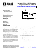
Table Of Contents

ADT6501/ADT6502/ADT6503/ADT6504 Data Sheet
Rev. B | Page 2 of 16
TABLE OF CONTENTS
Features .............................................................................................. 1
Applications ....................................................................................... 1
Functional Block Diagram .............................................................. 1
General Description ......................................................................... 1
Product Highlights ........................................................................... 1
Revision History ............................................................................... 2
Specifications ..................................................................................... 3
Absolute Maximum Ratings ............................................................ 4
ESD Caution .................................................................................. 4
Pin Configurations and Function Descriptions ........................... 5
Typical Performance Characteristics ............................................. 6
Theory of Operation ........................................................................ 8
Circuit Information ...................................................................... 8
Converter Details ..........................................................................8
Factory-Programmed Threshold Range ....................................8
Hysteresis Input .............................................................................8
Temperature Conversion ..............................................................8
Application Information ................................................................ 10
Thermal Response Time ........................................................... 10
Self-Heating Effects .................................................................... 10
Supply Decoupling ..................................................................... 10
Temperature Monitoring ........................................................... 10
Typical Application Circuits ......................................................... 11
Outline Dimensions ....................................................................... 13
Ordering Guide .......................................................................... 13
REVISION HISTORY
9/12—Rev. A to Rev. B
Change to Supply Current Parameter, Table 1 .............................. 3
Updated Outline Dimensions ....................................................... 13
1/08—Rev. 0 to Rev. A
Added ADT6503 and ADT6504 ....................................... Universal
Changes to Features .......................................................................... 1
Changes to Product Highlights ....................................................... 1
Changes to Table 1 ............................................................................. 3
Changes to Typical Performance Characteristics ......................... 6
Changes to Ordering Guide .......................................................... 13
9/
07—Revision 0: Initial Version