
Datasheet
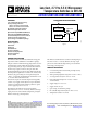
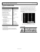
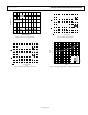
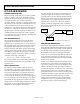
Table Of Contents

ADT6501/ADT6502/ADT6503/ADT6504 Data Sheet
Rev. B | Page 4 of 16
ABSOLUTE MAXIMUM RATINGS
Table 2.
Parameter Rating
V
CC
to GND −0.3 V to +7 V
HYST Input Voltage to GND
−0.3 V to V
CC
+ 0.3 V
Open-Drain Output Voltage to GND −0.3 V to +7 V
Push-Pull Output Voltage to GND −0.3 V to V
CC
+ 0.3 V
Input Current on All Pins 20 mA
Output Current on All Pins 20 mA
Operating Temperature Range
−55°C to +125°C
Storage Temperature Range −65°C to +160°C
Maximum Junction Temperature, T
JMAX
150.7°C
5-Lead SOT-23 (RJ-5)
Power Dissipation
1
W
MAX
= (T
JMAX
− T
A
2
)/θ
JA
Thermal Impedance
3
θ
JA
, Junction-to-Ambient (Still Air)
240°C/W
IR Reflow Soldering
(RoHS Compliant Package)
Peak Temperature 260°C (+0°C)
Time at Peak Temperature 20 sec to 40 sec
Ramp-Up Rate 3°C/sec maximum
Ramp-Down Rate
−6°C/sec maximum
Time 25°C to Peak Temperature 8 minute maximum
1
Values relate to package being used on a standard 2-layer PCB. This gives a
worst case θ
JA
. Refer to Figure 2 for a plot of maximum power dissipation vs.
ambient temperature (T
A
).
2
T
A
= ambient temperature.
3
Junction-to-case resistance is applicable to components featuring a
preferential flow direction, for example, components mounted on a
heat sink. Junction-to-ambient resistance is more useful for air-cooled,
PCB-mounted components.
Stresses above those listed under Absolute Maximum Ratings
may cause permanent damage to the device. This is a stress
rating only; functional operation of the device at these or any
other conditions above those indicated in the operational
section of this specification is not implied. Exposure to absolute
maximum rating conditions for extended periods may affect
device reliability.
Figure 2. SOT-23 Maximum Power Dissipation vs. Temperature
ESD CAUTION
0.9
0
125
TEMPERATURE (°C)
MAXIMUM POWER DISSIPATION (W)
06096-002
0.8
0.7
0.6
0.5
0.4
0.3
0.2
0.1
–55
–50
–40
–30
–20
–10
0
10
20
30
40
50
60
70
80
90
100
110
120
SOT-23 PD @ 125°C = 0.107W