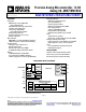
Precision Analog Microcontroller, 12-Bit Analog I/O, ARM7TDMI MCU ADuC7019/20/21/22/24/25/26/27/28/29 Data Sheet FEATURES On-chip peripherals UART, 2× I2C® and SPI serial I/O Up to 40-pin GPIO port1 4× general-purpose timers Wake-up and watchdog timers (WDT) Power supply monitor 3-phase, 16-bit PWM generator1 Programmable logic array (PLA) External memory interface, up to 512 kB1 Power Specified for 3 V operation Active mode: 11 mA @ 5 MHz, 40 mA @ 41.
ADuC7019/20/21/22/24/25/26/27/28/29 Data Sheet TABLE OF CONTENTS Features .............................................................................................. 1 Calibration................................................................................... 50 Applications ....................................................................................... 1 Temperature Sensor ................................................................... 50 Functional Block Diagram ...................
Data Sheet ADuC7019/20/21/22/24/25/26/27/28/29 REVISION HISTORY 5/13—Rev. E to Rev. F Changes to Figure 1........................................................................... 1 Added Figure 2 to Figure 10; Renumbered Sequentially ............. 4 Changes to Figure 19; Added Figure 20 .......................................21 Changes to EPAD Note in Figure 21 and Figure 22 ..................... 22 Changes to EPAD Note in Table 11....................................................
ADuC7019/20/21/22/24/25/26/27/28/29 Data Sheet GENERAL DESCRIPTION The devices operate from an on-chip oscillator and a PLL generating an internal high frequency clock of 41.78 MHz (UCLK). This clock is routed through a programmable clock divider from which the MCU core clock operating frequency is generated. The microcontroller core is an ARM7TDMI®, 16-bit/32-bit RISC machine, which offers up to 41 MIPS peak performance.
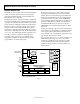
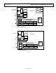
Data Sheet ADuC7019/20/21/22/24/25/26/27/28/29 ADC0 TO ADC7, ADC12 TO ADC13 1MSPS 12-BIT ADC MUX ADuC7021 12-BIT DAC DAC0 12-BIT DAC DAC1 TEMP SENSOR CMP0 CMP1 BAND GAP REF CMPOUT VREF OSC AND PLL XCLKO 2k × 32 SRAM 31k × 16 FLASH/EEPROM PLA PSM RST 3-PHASE PWM ARM7TDMI-BASED MCU WITH ADDITIONAL PERIPHERALS 4 GENERALPURPOSE TIMERS POR SERIAL I/O UART, SPI, I2C (SEE NOTE 1) GPIO JTAG 04955-102 XCLKI NOTES 1. SEE APPLICATION NOTE AN-798. Figure 3.
ADuC7019/20/21/22/24/25/26/27/28/29 ADC0 TO ADC9, ADC12, ADC13 MUX 1MSPS 12-BIT ADC Data Sheet ADuC7024 12-BIT DAC DAC0 12-BIT DAC DAC1 TEMP SENSOR CMP0 CMP1 BAND GAP REF CMPOUT VREF OSC AND PLL ARM7TDMI-BASED MCU WITH ADDITIONAL PERIPHERALS XCLKO PLA PSM RST 2k × 32 SRAM 31k × 16 FLASH/EEPROM 4 GENERALPURPOSE TIMERS POR SERIAL I/O UART, SPI, I2C (SEE NOTE 1) GPIO PWM0H PWM0L PWM1H PWM1L PWM2H PWM2L JTAG 04955-104 XCLKI 3-PHASE PWM NOTES 1. SEE APPLICATION NOTE AN-798. Figure 5.
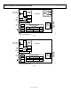
ADuC7019/20/21/22/24/25/26/27/28/29 MUX ADC0 TO ADC15 1MSPS 12-BIT ADC ADuC7026 TEMP SENSOR CMP0 CMP1 BAND GAP REF CMPOUT 12-BIT DAC DAC0 12-BIT DAC DAC1 12-BIT DAC DAC2 12-BIT DAC DAC3 VREF XCLKI OSC AND PLL PLA PSM RST 2k × 32 SRAM 31k × 16 FLASH/EEPROM 4 GENERALPURPOSE TIMERS POR 3-PHASE PWM ARM7TDMI-BASED MCU WITH ADDITIONAL PERIPHERALS XCLKO SERIAL I/O UART, SPI, I2C GPIO JTAG PWM0H PWM0L PWM1H PWM1L PWM2H PWM2L EXT. MEMORY INTERFACE 04955-106 Data Sheet Figure 7.
ADuC7019/20/21/22/24/25/26/27/28/29 ADC0 TO ADC7, ADC12 TO ADC15 MUX 1MSPS 12-BIT ADC Data Sheet ADuC7028 TEMP SENSOR CMP0 CMP1 BAND GAP REF CMPOUT 12-BIT DAC DAC0 12-BIT DAC DAC1 12-BIT DAC DAC2 12-BIT DAC DAC3 VREF OSC AND PLL PLA PSM RST 2k × 32 SRAM 31k × 16 FLASH/EEPROM GPIO SERIAL I/O UART, SPI, I2C JTAG 4 GENERALPURPOSE TIMERS POR 3-PHASE PWM ARM7TDMI-BASED MCU WITH ADDITIONAL PERIPHERALS 04955-108 XCLKI XCLKO PWM0H PWM0L PWM1H PWM1L PWM2H PWM2L Figure 9.
Data Sheet ADuC7019/20/21/22/24/25/26/27/28/29 25 54 28 27 37 ADuC7026* ADC0 77 ADC1 78 12-BIT SAR ADC 1MSPS ADC2/CMP0 79 ADC3/CMP1 80 ADC CONTROL ADC4 1 75 70 69 12-BIT VOLTAGE OUTPUT DAC BUF 10 DAC0*/ADC12 12-BIT VOLTAGE OUTPUT DAC BUF 11 DAC1*/ADC13 12-BIT VOLTAGE OUTPUT DAC BUF 12 DAC2*/ADC14 12-BIT VOLTAGE OUTPUT DAC BUF 13 DAC3*/ADC15 DAC CONTROL ADC5 2 ADC6 3 MUX ADC7 4 ADC8 5 ADC9 6 ADC10 7 ADC11 76 ADCNEG DAC REF RST 26 DACV DD LVDD 53 DACGND DGND 74 IOVD
ADuC7019/20/21/22/24/25/26/27/28/29 Data Sheet SPECIFICATIONS AVDD = IOVDD = 2.7 V to 3.6 V, VREF = 2.5 V internal reference, fCORE = 41.78 MHz, TA = −40°C to +125°C, unless otherwise noted. Table 1.
Data Sheet Parameter DAC AC CHARACTERISTICS Voltage Output Settling Time Digital-to-Analog Glitch Energy COMPARATOR Input Offset Voltage Input Bias Current Input Voltage Range Input Capacitance Hysteresis4, 6 ADuC7019/20/21/22/24/25/26/27/28/29 Min Input Capacitance LOGIC INPUTS3 VINL, Input Low Voltage VINH, Input High Voltage LOGIC OUTPUTS VOH, Output High Voltage VOL, Output Low Voltage11 CRYSTAL INPUTS XCLKI and XCLKO Logic Inputs, XCLKI Only VINL, Input Low Voltage VINH, Input High Voltage XCLKI Inp
ADuC7019/20/21/22/24/25/26/27/28/29 Parameter MCU CLOCK RATE From 32 kHz Internal Oscillator From 32 kHz External Crystal Using an External Clock Min DACVDD Current15 Digital Power Supply Current IOVDD Current in Normal Mode IOVDD Current in Pause Mode IOVDD Current in Sleep Mode Additional Power Supply Currents ADC DAC ESD TESTS HBM Passed Up To FCIDM Passed Up To Max Unit Test Conditions/Comments 44 41.78 kHz MHz MHz MHz CD12 = 7 CD12 = 0 TA = 85°C TA = 125°C Core clock = 41.78 MHz 326 41.78 0.
Data Sheet ADuC7019/20/21/22/24/25/26/27/28/29 TIMING SPECIFICATIONS Table 2.
ADuC7019/20/21/22/24/25/26/27/28/29 Data Sheet Table 3.
Data Sheet ADuC7019/20/21/22/24/25/26/27/28/29 Table 4. I2C Timing in Fast Mode (400 kHz) Parameter tL tH tSHD tDSU tDHD tRSU tPSU tBUF tR tF tSUP 1 Description SCL low pulse width1 SCL high pulse width1 Start condition hold time Data setup time Data hold time Setup time for repeated start Stop condition setup time Bus-free time between a stop condition and a start condition Rise time for both SCL and SDA Fall time for both SCL and SDA Pulse width of spike suppressed Min 200 100 300 100 0 100 100 1.
ADuC7019/20/21/22/24/25/26/27/28/29 Data Sheet Table 6. SPI Master Mode Timing (Phase Mode = 1) Parameter tSL tSH tDAV tDSU tDHD tDF tDR tSR tSF 2 Min Typ (SPIDIV + 1) × tHCLK (SPIDIV + 1) × tHCLK Max 25 1 × tUCLK 2 × tUCLK 5 5 5 5 12.5 12.5 12.5 12.5 tHCLK depends on the clock divider or CD bits in the POWCONMMR. tHCLK = tUCLK/2CD; see Figure 67. tUCLK = 23.9 ns. It corresponds to the 41.78 MHz internal clock from the PLL before the clock divider; see Figure 67.
Data Sheet ADuC7019/20/21/22/24/25/26/27/28/29 Table 7. SPI Master Mode Timing (Phase Mode = 0) Parameter tSL tSH tDAV tDOSU tDSU tDHD tDF tDR tSR tSF 2 Min Typ (SPIDIV + 1) × tHCLK (SPIDIV + 1) × tHCLK Max 25 75 1 × tUCLK 2 × tUCLK 5 5 5 5 12.5 12.5 12.5 12.5 Unit ns ns ns ns ns ns ns ns ns ns tHCLK depends on the clock divider or CD bits in the POWCONMMR. tHCLK = tUCLK/2CD; see Figure 67. tUCLK = 23.9 ns. It corresponds to the 41.
ADuC7019/20/21/22/24/25/26/27/28/29 Data Sheet Table 8.
Data Sheet ADuC7019/20/21/22/24/25/26/27/28/29 Table 9.
ADuC7019/20/21/22/24/25/26/27/28/29 Data Sheet ABSOLUTE MAXIMUM RATINGS AGND = REFGND = DACGND = GNDREF, TA = 25°C, unless otherwise noted. Table 10.
Data Sheet ADuC7019/20/21/22/24/25/26/27/28/29 PIN CONFIGURATIONS AND FUNCTION DESCRIPTIONS 40 39 38 37 36 35 34 33 32 31 ADC2/CMP0 ADC1 ADC0 AVDD AGND VREF P4.2/PLAO[10] P1.0/T1/SPM0/PLAI[0] P1.1/SPM1/PLAI[1] P1.2/SPM2/PLAI[2] ADuC7019/ADuC7020/ADuC7021/ADuC7022 ADuC7019 TOP VIEW (Not to Scale) 30 29 28 27 26 25 24 23 22 21 P1.3/SPM3/PLAI[3] P1.4/SPM4/PLAI[4]/IRQ2 P1.5/SPM5/PLAI[5]/IRQ3 P1.6/SPM6/PLAI[6] P1.7/SPM7/PLAO[0] XCLKI XCLKO P0.7/ECLK/XCLK/SPM8/PLAO[4] P2.0/SPM9/PLAO[5]/CONVSTART IRQ1/P0.
Data Sheet 40 39 38 37 36 35 34 33 32 31 ADC3/CMP1 ADC2/CMP0 ADC1 ADC0 AVDD AGND VREF P1.0/T1/SPM0/PLAI[0] P1.1/SPM1/PLAI[1] P1.2/SPM2/PLAI[2] ADuC7019/20/21/22/24/25/26/27/28/29 PIN 1 INDICATOR ADuC7021 TOP VIEW (Not to Scale) 30 29 28 27 26 25 24 23 22 21 P1.3/SPM3/PLAI[3] P1.4/SPM4/PLAI[4]/IRQ2 P1.5/SPM5/PLAI[5]/IRQ3 P1.6/SPM6/PLAI[6] P1.7/SPM7/PLAO[0] XCLKI XCLKO P0.7/ECLK/XCLK/SPM8/PLAO[4] P2.0/SPM9/PLAO[5]/CONVSTART IRQ1/P0.5/ADCBUSY/PLAO[2] NOTES 1.
Data Sheet ADuC7019/20/21/22/24/25/26/27/28/29 Table 11. Pin Function Descriptions (ADuC7019/ADuC7020/ADuC7021/ADuC7022) Pin No. 7019/7020 7021 38 37 39 38 40 39 1 40 7022 36 37 38 39 Mnemonic ADC0 ADC1 ADC2/CMP0 ADC3/CMP1 2 ‒ 1 2 40 1 ADC4 ADC5 Description Single-Ended or Differential Analog Input 0. Single-Ended or Differential Analog Input 1. Single-Ended or Differential Analog Input 2/Comparator Positive Input.
ADuC7019/20/21/22/24/25/26/27/28/29 Pin No. 7019/7020 7021 22 22 7022 21 Mnemonic P2.0/SPM9/PLAO[5]/CONVSTART 23 23 22 P0.7/ECLK/XCLK/SPM8/PLAO[4] 24 25 24 25 23 24 XCLKO XCLKI 26 26 25 P1.7/SPM7/PLAO[0] 27 27 26 P1.6/SPM6/PLAI[6] 28 28 27 P1.5/SPM5/PLAI[5]/IRQ3 29 29 28 P1.4/SPM4/PLAI[4]/IRQ2 30 30 29 P1.3/SPM3/PLAI[3] 31 31 30 P1.2/SPM2/PLAI[2] 32 32 31 P1.1/SPM1/PLAI[1] 33 33 32 P1.0/T1/SPM0/PLAI[0] 34 ‒ ‒ P4.
Data Sheet ADuC7019/20/21/22/24/25/26/27/28/29 64 63 62 61 60 59 58 57 56 55 54 53 52 51 50 49 ADC3/CMP1 ADC2/CMP0 ADC1 ADC0 DACV DD AVDD AGND DACGND DAC REF VREF P4.5/PLAO[13] P4.4/PLAO[12] P4.3/PLAO[11] P4.2/PLAO[10] P1.0/T1/SPM0/PLAI[0] P1.1/SPM1/PLAI[1] ADuC7024/ADuC7025 1 2 3 4 5 6 7 8 9 10 11 12 13 14 15 16 PIN 1 INDICATOR ADuC7024/ ADuC7025 TOP VIEW (Not to Scale) 48 47 46 45 44 43 42 41 40 39 38 37 36 35 34 33 P1.2/SPM2/PLAI[2] P1.3/SPM3/PLAI[3] P1.4/SPM4/PLAI[4]/IRQ2 P1.
ADuC7019/20/21/22/24/25/26/27/28/29 Data Sheet Table 12. Pin Function Descriptions (ADuC7024/ADuC7025 64-Lead LFCSP_VQ and 64-Lead LQFP) Pin No. 1 2 3 4 5 6 7 Mnemonic ADC4 ADC5 ADC6 ADC7 ADC8 ADC9 GNDREF 8 ADCNEG 9 DAC0/ADC12 10 DAC1/ADC13 11 12 13 14 15 TMS TDI P4.6/PLAO[14] P4.7/PLAO[15] BM/P0.0/CMPOUT/PLAI[7] 16 P0.6/T1/MRST/PLAO[3] 17 18 19 20 21 TCK TDO IOGND IOVDD LVDD 22 23 DGND P3.0/PWM0H/PLAI[8] 24 P3.1/PWM0L/PLAI[9] 25 P3.2/PWM1H/PLAI[10] 26 P3.
Data Sheet Pin No. 37 Mnemonic P3.6/PWMTRIP/PLAI[14] 38 P3.7/PWMSYNC/PLAI[15] 39 P1.7/SPM7/PLAO[0] 40 P1.6/SPM6/PLAI[6] 41 42 43 44 45 IOGND IOVDD P4.0/PLAO[8] P4.1/PLAO[9] P1.5/SPM5/PLAI[5]/IRQ3 46 P1.4/SPM4/PLAI[4]/IRQ2 47 P1.3/SPM3/PLAI[3] 48 P1.2/SPM2/PLAI[2] 49 P1.1/SPM1/PLAI[1] 50 P1.0/T1/SPM0/PLAI[0] 51 52 53 54 55 P4.2/PLAO[10] P4.3/PLAO[11] P4.4/PLAO[12] P4.
ADuC7019/20/21/22/24/25/26/27/28/29 Data Sheet 80 79 78 77 76 75 74 73 72 71 70 69 68 67 66 65 64 63 62 61 ADC3/CMP1 ADC2/CMP0 ADC1 ADC0 ADC11 DACV DD AVDD AVDD AGND AGND DACGND DACREF VREF REFGND P4.5/AD13/PLAO[13] P4.4/AD12/PLAO[12] P4.3/AD11/PLAO[11] P4.2/AD10/PLAO[10] P1.0/T1/SPM0/PLAI[0] P1.1/SPM1/PLAI[1] ADuC7026/ADuC7027 1 2 3 4 5 6 7 8 9 10 11 12 13 14 15 16 17 18 19 20 PIN 1 INDICATOR ADuC7026/ ADuC7027 TOP VIEW (Not to Scale) 60 59 58 57 56 55 54 53 52 51 50 49 48 47 46 45 44 43 42 41 P1.
Data Sheet Pin No. 18 Mnemonic P4.6/AD14/PLAO[14] 19 P4.7/AD15/PLAO[15] 20 BM/P0.0/CMPOUT/PLAI[7]/MS0 21 P0.6/T1/MRST/PLAO[3] 22 23 24 TCK TDO P0.2/PWM2L/BHE 25 26 27 IOGND IOVDD LVDD 28 29 DGND P3.0/AD0/PWM0H/PLAI[8] 30 P3.1/AD1/PWM0L/PLAI[9] 31 P3.2/AD2/PWM1H/PLAI[10] 32 P3.3/AD3/PWM1L/PLAI[11] 33 P2.4/PWM0H/MS0 34 35 P0.3/TRST/A16/ADCBUSY P2.5/PWM0L/MS1 36 P2.6/PWM1H/MS2 37 38 RST P3.4/AD4/PWM2H/PLAI[12] 39 P3.5/AD5/PWM2L/PLAI[13] 40 IRQ0/P0.
ADuC7019/20/21/22/24/25/26/27/28/29 Pin No. 46 Mnemonic P3.6/AD6/PWMTRIP/PLAI[14] 47 P3.7/AD7/PWMSYNC/PLAI[15] 48 P2.7/PWM1L/MS3 49 P2.1/WS/PWM0H/PLAO[6] 50 P2.2/RS/PWM0L/PLAO[7] 51 P1.7/SPM7/PLAO[0] 52 P1.6/SPM6/PLAI[6] 53 54 55 IOGND IOVDD P4.0/AD8/PLAO[8] 56 P4.1/AD9/PLAO[9] 57 P1.5/SPM5/PLAI[5]/IRQ3 58 P1.4/SPM4/PLAI[4]/IRQ2 59 P1.3/SPM3/PLAI[3] 60 P1.2/SPM2/PLAI[2] 61 P1.1/SPM1/PLAI[1] 62 P1.0/T1/SPM0/PLAI[0] 63 P4.2/AD10/PLAO[10] 64 P4.3/AD11/PLAO[11] 65 P4.
Data Sheet ADuC7019/20/21/22/24/25/26/27/28/29 ADUC7028 8 7 6 5 4 3 2 1 A B C D E F H BOTTOM VIEW (Not to Scale) 04955-086 G Figure 26. 64-Ball CSP_BGA Pin Configuration (ADuC7028) Table 14. Pin Function Descriptions (ADuC7028) Ball No. A1 A2 A3 A4 A5 A6 A7 Mnemonic ADC3/CMP1 DACVDD AVDD AGND DACGND P4.2/PLAO[10] P1.1/SPM1/PLAI[1] A8 P1.2/SPM2/PLAI[2] B1 B2 B3 B4 B5 ADC4 ADC2/CMP0 ADC1 DACREF VREF B6 P1.0/T1/SPM0/PLAI[0] B7 P1.4/SPM4/PLAI[4]/IRQ2 B8 P1.
ADuC7019/20/21/22/24/25/26/27/28/29 Ball No. D7 Mnemonic P1.6/SPM6/PLAI[6] D8 E1 E2 E3 E4 IOVDD DAC3/ADC15 DAC2/ADC14 DAC1/ADC13 P3.0/PWM0H/PLAI[8] E5 P3.2/PWM1H/PLAI[10] E6 P1.5/SPM5/PLAI[5]/IRQ3 E7 P3.7/PWMSYNC/PLAI[15] E8 F1 F2 XCLKI P4.6/PLAO[14] TDI F3 F4 DAC0/ADC12 P3.1/PWM0L/PLAI[9] F5 P3.3/PWM1L/PLAI[11] F6 F7 RST P0.7/ECLK/XCLK/SPM8/PLAO[4] F8 G1 XCLKO BM/P0.0/CMPOUT/PLAI[7] G2 G3 G4 G5 P4.7/PLAO[15] TMS TDO P0.3/TRST/ADCBUSY G6 P3.4/PWM2H/PLAI[12] G7 P3.
Data Sheet ADuC7019/20/21/22/24/25/26/27/28/29 ADUC7029 7 6 5 4 3 2 1 A B C D E G BOTTOM VIEW (Not to Scale) 04955-088 F Figure 27. 49-Ball CSP_BGA Pin Configuration (ADuC7029) Table 15. Pin Function Descriptions (ADuC7029) Ball No. A1 A2 A3 A4 A5 Mnemonic ADC3/CMP1 ADC1 ADC0 AVDD VREF A6 P1.0/T1/SPM0/PLAI[0] A7 P1.1/SPM1/PLAI[1] B1 B2 B3 B4 B5 B6 ADC6 ADC5 ADC4 AGND DACREF P1.4/SPM4/PLAI[4]/IRQ2 B7 P1.3/SPM3/PLAI[3] C1 GNDREF C2 C3 C4 C5 AGND ADC2/CMP0 IOGND P1.
ADuC7019/20/21/22/24/25/26/27/28/29 Ball No. E1 E2 Mnemonic TMS BM/P0.0/CMPOUT/PLAI[7] E3 E4 E5 DAC2/ADC14 IOVDD P3.2/PWM1H/PLAI[10] E6 P3.5/PWM2L/PLAI[13] E7 P0.7/ECLK/XCLK/SPM8/PLAO[4] F1 F2 TDI P0.6/T1/MRST/PLAO[3] F3 F4 IOGND P3.1/PWM0L/PLAI[9] F5 P3.0/PWM0H/PLAI[8] F6 F7 RST P2.0/SPM9/PLAO[5]/CONVSTART G1 G2 G3 TCK TDO LVDD G4 G5 DGND P0.3/TRST/ADCBUSY G6 IRQ0/P0.4/PWMTRIP/PLAO[1] G7 IRQ1/P0.5/ADCBUSY/PLAO[2] Data Sheet Description JTAG Test Port Input, Test Mode Select.
Data Sheet ADuC7019/20/21/22/24/25/26/27/28/29 TYPICAL PERFORMANCE CHARACTERISTICS 1.0 1.0 fS = 774kSPS fS = 774kSPS 0.8 0.4 0.2 0.2 (LSB) 0.6 0.4 0 0 –0.2 –0.4 –0.4 –0.6 –0.6 04955-075 –0.2 –0.8 0 1000 2000 ADC CODES 3000 –0.8 –1.0 4000 0 Figure 28. Typical INL Error, fS = 774 kSPS 0.6 0.6 0.4 0.4 0.2 0.2 (LSB) 0.8 0 0 –0.2 –0.4 –0.4 –0.6 –0.6 04955-077 –0.2 0 1000 2000 ADC CODES 3000 04955-076 (LSB) 4000 fS = 1MSPS 0.8 –0.8 –0.8 –1.
ADuC7019/20/21/22/24/25/26/27/28/29 Data Sheet –76 75 9000 8000 70 –78 SNR 7000 65 SNR (dB) FREQUENCY 5000 4000 60 –82 THD 55 THD (dB) –80 6000 –84 3000 50 2000 1161 1162 BIN 40 1163 1.0 Figure 34. Code Histogram Plot, fs = 774 kSPS, VIN = 0.7 V 1.5 2.0 2.5 EXTERNAL REFERENCE (V) –88 3.0 04955-070 0 –86 45 04955-073 1000 Figure 37. Typical Dynamic Performance vs. VREF 1500 0 fS = 774kSPS, SNR = 69.3dB, THD = –80.8dB, PHSN = –83.
Data Sheet ADuC7019/20/21/22/24/25/26/27/28/29 12.05 1.4 12.00 1.2 11.95 1.0 11.90 0.8 (mA) (mA) 11.85 11.80 0.6 11.75 11.70 0.4 11.65 –40 0 25 85 TEMPERATURE (°C) 0 125 Figure 40. Current Consumption vs. Temperature @ CD = 3 04955-083 11.55 0.2 04955-081 11.60 –40 0 25 85 TEMPERATURE (°C) 125 Figure 42. Current Consumption vs. Temperature in Sleep Mode 7.85 37.4 7.80 37.2 7.75 37.0 (mA) 7.65 7.60 7.55 36.8 36.6 7.50 7.45 7.
ADuC7019/20/21/22/24/25/26/27/28/29 Data Sheet TERMINOLOGY ADC SPECIFICATIONS Integral Nonlinearity (INL) The maximum deviation of any code from a straight line passing through the endpoints of the ADC transfer function. The endpoints of the transfer function are zero scale, a point ½ LSB below the first code transition, and full scale, a point ½ LSB above the last code transition.
Data Sheet ADuC7019/20/21/22/24/25/26/27/28/29 OVERVIEW OF THE ARM7TDMI CORE The ARM7® core is a 32-bit reduced instruction set computer (RISC). It uses a single 32-bit bus for instruction and data. The length of the data can be eight bits, 16 bits, or 32 bits. The length of the instruction word is 32 bits. The ARM7TDMI is an ARM7 core with four additional features. T support for the thumb (16-bit) instruction set. D support for debug. M support for long multiplications.
ADuC7019/20/21/22/24/25/26/27/28/29 More information relative to the programmer’s model and the ARM7TDMI core architecture can be found in the following materials from ARM: • • DDI0029G, ARM7TDMI Technical Reference Manual DDI-0100, ARM Architecture Reference Manual INTERRUPT LATENCY The worst-case latency for a fast interrupt request (FIQ) consists of the following: • • • • The longest time the request can take to pass through the synchronizer The time for the longest instruction to complete (the longe
Data Sheet ADuC7019/20/21/22/24/25/26/27/28/29 MEMORY ORGANIZATION The ADuC7019/20/21/22/24/25/26/27/28/29 incorporate two separate blocks of memory: 8 kB of SRAM and 64 kB of on-chip Flash/EE memory. The 62 kB of on-chip Flash/EE memory is available to the user, and the remaining 2 kB are reserved for the factory-configured boot page. These two blocks are mapped as shown in Figure 45.
ADuC7019/20/21/22/24/25/26/27/28/29 0xFFFFFFFF Data Sheet Table 16.
Data Sheet Access Address Name Byte Type Reference Address Base = 0xFFFF0480 0x048C REFCON 1 R/W ADuC7019/20/21/22/24/25/26/27/28/29 Default Value Page 0x00 50 ADC Address Base = 0xFFFF0500 0x0500 ADCCON 2 R/W 0x0504 ADCCP 1 R/W 0x0508 ADCCN 1 R/W 0x050C ADCSTA 1 R 0x0510 ADCDAT 4 R 0x0514 ADCRST 1 R/W 0x0530 ADCGN 2 R/W 0x0534 ADCOF 2 R/W 0x0600 0x00 0x01 0x00 0x00000000 0x00 0x0200 0x0200 46 47 47 48 48 48 48 48 DAC Address Base = 0xFFFF0600 0x0600 DAC0CON 1 R/W 0x0604 DAC0DAT 4 R/W 0x0608 DAC1CON
ADuC7019/20/21/22/24/25/26/27/28/29 Address Name Byte PLA Base Address = 0xFFFF0B00 0x0B00 PLAELM0 2 0x0B04 PLAELM1 2 0x0B08 PLAELM2 2 0x0B0C PLAELM3 2 0x0B10 PLAELM4 2 0x0B14 PLAELM5 2 0x0B18 PLAELM6 2 0x0B1C PLAELM7 2 0x0B20 PLAELM8 2 0x0B24 PLAELM9 2 0x0B28 PLAELM10 2 0x0B2C PLAELM11 2 0x0B30 PLAELM12 2 0x0B34 PLAELM13 2 0x0B38 PLAELM14 2 0x0B3C PLAELM15 2 0x0B40 PLACLK 1 0x0B44 PLAIRQ 4 0x0B48 PLAADC 4 0x0B4C PLADIN 4 0x0B50 PLADOUT 4 0x0B54 PLALCK 1 Access Type Default Value Page R/W R/W R/W R/W R/
Data Sheet ADuC7019/20/21/22/24/25/26/27/28/29 ADC CIRCUIT OVERVIEW The analog-to-digital converter (ADC) incorporates a fast, multichannel, 12-bit ADC. It can operate from 2.7 V to 3.6 V supplies and is capable of providing a throughput of up to 1 MSPS when the clock source is 41.78 MHz. This block provides the user with a multichannel multiplexer, a differential track-and-hold, an on-chip reference, and an ADC.
ADuC7019/20/21/22/24/25/26/27/28/29 Data Sheet ACQ TYPICAL OPERATION Once configured via the ADC control and channel selection registers, the ADC converts the analog input and provides a 12-bit result in the ADC data register. SIGN BITS ADC BUSY DATA ADCDAT 0 12-BIT ADC RESULT ADCSTA = 0 ADCSTA = 1 04955-015 16 15 CONVSTART 04955-014 27 WRITE ADC CLOCK The top four bits are the sign bits. The 12-bit result is placed from Bit 16 to Bit 27, as shown in Figure 51.
Data Sheet ADuC7019/20/21/22/24/25/26/27/28/29 Table 18. ADCCON MMR Bit Designations Bit 15:13 12:10 Value 000 001 010 011 100 101 9:8 00 01 10 11 7 6 5 4:3 00 01 10 11 2:0 000 001 010 011 100 101 Other Description Reserved. ADC clock speed. fADC/1. This divider is provided to obtain 1 MSPS ADC with an external clock <41.78 MHz. fADC/2 (default value). fADC/4. fADC/8. fADC/16. fADC/32. ADC acquisition time. Two clocks. Four clocks. Eight clocks (default value). 16 clocks. Enable start conversion.
ADuC7019/20/21/22/24/25/26/27/28/29 Data Sheet Table 22. ADCCN MMR Bit Designation Table 27. ADCOF Register Bit 7:5 4:0 Name ADCOF Table 23. ADCSTA Register Name ADCSTA Address 0xFFFF050C Default Value 0x00 Access R ADCSTA is an ADC status register that indicates when an ADC conversion result is ready. The ADCSTA register contains only one bit, ADCReady (Bit 0), representing the status of the ADC. This bit is set at the end of an ADC conversion, generating an ADC interrupt.
Data Sheet ADuC7019/20/21/22/24/25/26/27/28/29 AVDD Pseudo Differential Mode In pseudo differential mode, Channel− is linked to the VIN− pin of the ADuC7019/20/21/22/24/25/26/27/28/29. SW2 switches between A (Channel−) and B (VREF). The VIN− pin must be connected to ground or a low voltage. The input signal on VIN+ can then vary from VIN− to VREF + VIN−. Note that VIN− must be chosen so that VREF + VIN− does not exceed AVDD.
ADuC7019/20/21/22/24/25/26/27/28/29 Table 28. VCM Ranges AVDD 3.3 V 3.0 V VREF 2.5 V 2.048 V 1.25 V 2.5 V 2.048 V 1.25 V VCM Min 1.25 V 1.024 V 0.75 V 1.25 V 1.024 V 0.75 V VCM Max 2.05 V 2.276 V 2.55 V 1.75 V 1.976 V 2.25 V Signal Peak-to-Peak 2.5 V 2.048 V 1.25 V 2.5 V 2.048 V 1.25 V Data Sheet ADCCP = 0x10; // Select Temperature Sensor as an // input to the ADC REFCON = 0x01; // connect internal 2.
Data Sheet ADuC7019/20/21/22/24/25/26/27/28/29 NONVOLATILE FLASH/EE MEMORY Like EEPROM, flash memory can be programmed in-system at a byte level, although it must first be erased. The erase is performed in page blocks. As a result, flash memory is often and more correctly referred to as Flash/EE memory. Overall, Flash/EE memory represents a step closer to the ideal memory device that includes nonvolatility, in-circuit programmability, high density, and low cost.
ADuC7019/20/21/22/24/25/26/27/28/29 Data Sheet SECURITY FLASH/EE CONTROL INTERFACE The 62 kB of Flash/EE memory available to the user can be read and write protected. Serial and JTAG programming use the Flash/EE control interface, which includes the eight MMRs outlined in this section. Bit 31 of the FEEPRO/FEEHIDE MMR (see Table 42) protects the 62 kB from being read through JTAG programming mode. The other 31 bits of this register protect writing to the flash memory.
Data Sheet ADuC7019/20/21/22/24/25/26/27/28/29 Table 35. FEECON Register Name FEECON Address 0xFFFFF808 Default Value 0x07 Access R/W FEECON is an 8-bit command register. The commands are described in Table 36.
ADuC7019/20/21/22/24/25/26/27/28/29 Data Sheet EXECUTION TIME FROM SRAM AND FLASH/EE RESET AND REMAP Execution from SRAM The ARM exception vectors are all situated at the bottom of the memory array, from Address 0x00000000 to Address 0x00000020, as shown in Figure 62. Fetching instructions from SRAM takes one clock cycle; the access time of the SRAM is 2 ns, and a clock cycle is 22 ns minimum.
Data Sheet ADuC7019/20/21/22/24/25/26/27/28/29 Reset Operation Table 46. RSTSTA Register There are four kinds of reset: external, power-on, watchdog expiration, and software force. The RSTSTA register indicates the source of the last reset, and RSTCLR allows clearing of the RSTSTA register. These registers can be used during a reset exception service routine to identify the source of the reset. If RSTSTA is null, the reset is external. Table 44.
ADuC7019/20/21/22/24/25/26/27/28/29 Data Sheet OTHER ANALOG PERIPHERALS DAC Table 51. DACxDAT Registers The ADuC7019/20/21/22/24/25/26/27/28/29 incorporate two, three, or four 12-bit voltage output DACs on-chip, depending on the model. Each DAC has a rail-to-rail voltage output buffer capable of driving 5 kΩ/100 pF. Name DAC0DAT DAC1DAT DAC2DAT DAC3DAT Each DAC has three selectable ranges: 0 V to VREF (internal band gap 2.5 V reference), 0 V to DACREF, and 0 V to AVDD.
Data Sheet ADuC7019/20/21/22/24/25/26/27/28/29 Linearity degradation near ground and AVDD is caused by saturation of the output amplifier, and a general representation of its effects (neglecting offset and gain error) is illustrated in Figure 64. The dotted line in Figure 64 indicates the ideal transfer function, and the solid line represents what the transfer function may look like with endpoint nonlinearities due to saturation of the output amplifier.
ADuC7019/20/21/22/24/25/26/27/28/29 Comparator Interface The comparator interface consists of a 16-bit MMR, CMPCON, which is described in Table 56. Table 55. CMPCON Register Name CMPCON Address 0xFFFF0444 Default Value 0x0000 Access R/W Table 56. CMPCON MMR Bit Descriptions Bit 15:11 10 Name CMPEN 9:8 CMPIN Value 00 01 10 11 7:6 CMPOC 00 01 10 11 5 4:3 CMPOL CMPRES 00 11 01/10 2 CMPHYST 1 CMPORI 0 CMPOFI Description Reserved. Comparator enable bit. Set by user to enable the comparator.
Data Sheet ADuC7019/20/21/22/24/25/26/27/28/29 Example source code Example source code t2val_old= T2VAL; t2val_old= T2VAL; T2LD = 5; T2LD = 5; TCON = 0x480; TCON = 0x480; while ((T2VAL == t2val_old) || (T2VAL > 3)) //ensures timer value loaded while ((T2VAL == t2val_old) || (T2VAL > 3)) //ensures timer value loaded IRQEN = 0x10; //enable T2 interrupt IRQEN = 0x10; //enable T2 interrupt PLLKEY1 = 0xAA; PLLCON = 0x01; PLLKEY2 = 0x55; PLLKEY1 = 0xAA; PLLCON = 0x03; //Select external clock PLLKEY2
ADuC7019/20/21/22/24/25/26/27/28/29 Data Sheet MMRs and Keys Table 63. POWCON Register The operating mode, clocking mode, and programmable clock divider are controlled via two MMRs: PLLCON (see Table 61) and POWCON (see Table 64). PLLCON controls the operating mode of the clock system, whereas POWCON controls the core clock frequency and the power-down mode. Name POWCON To prevent accidental programming, a certain sequence (see Table 65) must be followed to write to the PLLCON and POWCON registers.
Data Sheet ADuC7019/20/21/22/24/25/26/27/28/29 DIGITAL PERIPHERALS 3-PHASE PWM Each ADuC7019/20/21/22/24/25/26/27/28/29 provides a flexible and programmable, 3-phase pulse-width modulation (PWM) waveform generator. It can be programmed to generate the required switching patterns to drive a 3-phase voltage source inverter for ac induction motor control (ACIM). Note that only active high patterns can be produced.
ADuC7019/20/21/22/24/25/26/27/28/29 DESCRIPTION OF THE PWM BLOCK A functional block diagram of the PWM controller is shown in Figure 68. The generation of the six output PWM signals on Pin PWM0H to Pin PWM2L is controlled by the following four important blocks: • • • The 3-phase PWM timing unit. The core of the PWM controller, this block generates three pairs of complemented and dead-time-adjusted, center-based PWM signals. This unit also generates the internal synchronization pulse, PWMSYNC.
Data Sheet ADuC7019/20/21/22/24/25/26/27/28/29 The PWMDAT1 register is a 10-bit register with a maximum value of 0x3FF (= 1023), which corresponds to a maximum programmed dead time of The advantage of double update mode is that lower harmonic voltages can be produced by the PWM process, and faster control bandwidths are possible. However, for a given PWM switching frequency, the PWMSYNC pulses occur at twice the rate in the double update mode.
ADuC7019/20/21/22/24/25/26/27/28/29 Both switching edges are moved by an equal amount (PWMDAT1 × tCORE) to preserve the symmetrical output patterns. Data Sheet In general, the on times of the PWM signals in double update mode can be defined as follows: On the high side Also shown are the PWMSYNC pulse and Bit 0 of the PWMSTA register, which indicates whether operation is in the first or second half cycle of the PWM period.
Data Sheet ADuC7019/20/21/22/24/25/26/27/28/29 PWMCH0 = PWMCH0 = PWMCH1 PWMCH1 Output Control Unit Following a reset, all six enable bits of the PWMEN register are cleared, and all PWM outputs are enabled by default. In a manner identical to the duty cycle registers, the PWMEN is latched on the rising edge of the PWMSYNC signal. As a result, changes to this register become effective only at the start of each PWM cycle in single update mode.
ADuC7019/20/21/22/24/25/26/27/28/29 The GDCLK value can range from 0 to 255, corresponding to a programmable chopping frequency rate of 40.8 kHz to 10.44 MHz for a 41.78 MHz core frequency. The gate drive features must be programmed before operation of the PWM controller and are typically not changed during normal operation of the PWM controller. Following a reset, all bits of the PWMCFG register are cleared so that high frequency chopping is disabled, by default.
Data Sheet ADuC7019/20/21/22/24/25/26/27/28/29 Table 70. PWMCFG Register Table 74. PWMDAT0 Register Name PWMCFG Address 0xFFFFFC10 Default Value 0x0000 Access R/W PWMCFG is a gate chopping register. Name PWMDAT0 Address 0xFFFFFC08 Table 75. PWMDAT1 Register Bit 15:10 9 8 7:0 Name PWMDAT1 CHOPLO CHOPHI GDCLK Description Reserved. Low-side gate chopping enable bit. High-side gate chopping enable bit. PWM gate chopping period (unsigned). Table 72.
ADuC7019/20/21/22/24/25/26/27/28/29 GPxCON are the Port x control registers, which select the function of each pin of Port x as described in Table 80. Table 78. GPIO Pin Function Descriptions Port 0 1 2 3 4 Pin P0.0 P0.1 P0.2 P0.3 P0.4 P0.5 P0.6 P0.7 P1.0 P1.1 P1.2 P1.3 P1.4 P1.5 P1.6 P1.7 00 GPIO GPIO GPIO GPIO GPIO/IRQ0 GPIO/IRQ1 GPIO/T1 GPIO GPIO/T1 GPIO GPIO GPIO GPIO/IRQ2 GPIO/IRQ3 GPIO GPIO P2.0 P2.1 P2.2 P2.3 P2.4 P2.5 P2.6 P2.7 P3.0 P3.1 P3.2 P3.3 P3.4 P3.5 P3.6 P3.7 P4.0 P4.1 P4.2 P4.3 P4.
Data Sheet ADuC7019/20/21/22/24/25/26/27/28/29 Table 83. GPIO Drive Strength Control Bits Descriptions Table 84. GPxPAR Control Bits Access Descriptions Control Bits Value 00 01 1x Bit 31 30 to 29 28 27 26 to 25 24 23 22 to 21 20 19 18 to 17 16 15 14 to 13 12 11 10 to 9 8 7 6 to 5 4 3 2 to 1 0 Description Medium drive strength. Low drive strength. High drive strength. 3.6 3.2 3.0 2.8 2.6 2.4 HIGH DRIVE STRENGTH MEDIUM DRIVE STRENGTH LOW DRIVE STRENGTH 2.2 2.
ADuC7019/20/21/22/24/25/26/27/28/29 Table 90. GPxCLR MMR Bit Descriptions Table 85. GPxDAT Registers Name GP0DAT GP1DAT GP2DAT GP3DAT GP4DAT 1 Address 0xFFFFF420 0xFFFFF430 0xFFFFF440 0xFFFFF450 0xFFFFF460 Data Sheet Default Value1 0x000000XX 0x000000XX 0x000000XX 0x000000XX 0x000000XX Access R/W R/W R/W R/W R/W X = 0, 1, 2, or 3. Bit 31:24 23:16 15:0 Description Reserved. Data Port x clear bit. Set to 1 by user to clear bit on Port x; also clears the corresponding bit in the GPxDAT MMR.
Data Sheet ADuC7019/20/21/22/24/25/26/27/28/29 The serial communication adopts an asynchronous protocol, which supports various word lengths, stop bits, and parity generation options selectable in the configuration register. Baud Rate Generation There are two ways of generating the UART baud rate, normal 450 UART baud rate generation and the fractional divider.
ADuC7019/20/21/22/24/25/26/27/28/29 Table 99. COMDIV1 Register Name COMDIV1 Address 0xFFFF0704 Table 104. COMCON1 Register Default Value 0x00 Access R/W COMDIV1 is a divisor latch (high byte) register. Address 0xFFFF0708 Name COMCON1 Access R Bit 7:5 4 Name 3 PEN 2 STOP 1 RTS 0 DTR LOOPBACK Table 101.
Data Sheet ADuC7019/20/21/22/24/25/26/27/28/29 Table 108. COMSTA1 Register Network Addressable UART Register Definitions Name COMSTA1 Address 0xFFFF0718 Default Value 0x00 Access R COMSTA1 is a modem status register. Table 109. COMSTA1 MMR Bit Descriptions Bit 7 6 5 4 3 Name DCD RI DSR CTS DDCD 2 TERI 1 DDSR 0 DCTS Description Data carrier detect. Ring indicator. Data set ready. Clear to send. Delta DCD. Set automatically if DCD changed state since last COMSTA1 read.
ADuC7019/20/21/22/24/25/26/27/28/29 MISO (Master In, Slave Out) Pin Table 116.
Data Sheet ADuC7019/20/21/22/24/25/26/27/28/29 SPI Registers Table 121. SPIRX Register The following MMR registers are used to control the SPI interface: SPISTA, SPIRX, SPITX, SPIDIV, and SPICON. Name SPIRX Address 0xFFFF0A00 Default Value 0x00 Access R SPISTA is an 8-bit read-only status register. Only Bit 1 or Bit 4 of this register generates an interrupt. Bit 6 of the SPICON register determines which bit generates the interrupt. Table 120.
ADuC7019/20/21/22/24/25/26/27/28/29 Data Sheet I2C-COMPATIBLE INTERFACES Slave Addresses The ADuC7019/20/21/22/24/25/26/27/28/29 support two licensed I2C interfaces. The I2C interfaces are both implemented as a hardware master and a full slave interface. Because the two I2C interfaces are identical, this data sheet describes only I2C0 in detail. Note that the two masters and one of the slaves have individual interrupts (see the Interrupt System section).
Data Sheet ADuC7019/20/21/22/24/25/26/27/28/29 Table 129. I2C0SSTA MMR Bit Descriptions Table 130. I2CxSRX Registers Bit 31:15 14 Value 13 12:11 00 01 10 11 10 9:8 00 01 10 11 7 6 5 4 3 2 1 0 Description Reserved. These bits should be written as 0. Start decode bit. Set by hardware if the device receives a valid start plus matching address. Cleared by an I2C stop condition or an I2C general call reset. Repeated start decode bit.
ADuC7019/20/21/22/24/25/26/27/28/29 Table 137. I2CxALT Registers Name I2C0ALT I2C1ALT Address 0xFFFF0828 0xFFFF0928 Data Sheet Table 138. I2CxCFG Registers Default Value 0x00 0x00 Access R/W R/W I2CxALT are hardware general call ID registers used in slave mode. Name I2C0CFG I2C1CFG Address 0xFFFF082C 0xFFFF092C Default Value 0x00 0x00 Access R/W R/W I2CxCFG are configuration registers. Table 139. I2C0CFG MMR Bit Descriptions Bit 31:5 14 13 12 11 10 9 8 7 6 5 4 3 2 1 0 Description Reserved.
Data Sheet ADuC7019/20/21/22/24/25/26/27/28/29 Table 140. I2CxDIV Registers Table 144. I2C0FSTA MMR Bit Descriptions Name I2C0DIV I2C1DIV Address 0xFFFF0830 0xFFFF0930 Default Value 0x1F1F 0x1F1F Access R/W R/W I2CxDIV are the clock divider registers. Bit 15:10 9 Access Type Value R/W Table 141.
ADuC7019/20/21/22/24/25/26/27/28/29 Data Sheet PROGRAMMABLE LOGIC ARRAY (PLA) Table 146. PLAELMx Registers Every ADuC7019/20/21/22/24/25/26/27/28/29 integrates a fully programmable logic array (PLA) that consists of two independent but interconnected PLA blocks. Each block consists of eight PLA elements, giving each part a total of 16 PLA elements.
Data Sheet ADuC7019/20/21/22/24/25/26/27/28/29 Table 148. PLACLK Register Name PLACLK Address 0xFFFF0B40 Default Value 0x00 Access R/W PLACLK is the clock selection for the flip-flops of Block 0 and Block 1. Note that the maximum frequency when using the GPIO pins as the clock input for the PLA blocks is 44 MHz.
ADuC7019/20/21/22/24/25/26/27/28/29 Table 156. PLADIN MMR Bit Descriptions Table 153. PLAADC Register Name PLAADC Address 0xFFFF0B48 Default Value 0x00000000 Access R/W PLAADC is the PLA source for the ADC start conversion signal. Value 3:0 0000 0001 1111 Description Reserved. ADC start conversion enable bit. Set by user to enable ADC start conversion from PLA. Cleared by user to disable ADC start conversion from PLA. ADC start conversion source. PLA Element 0. PLA Element 1. PLA Element 15.
Data Sheet ADuC7019/20/21/22/24/25/26/27/28/29 PROCESSOR REFERENCE PERIPHERALS IRQ INTERRUPT SYSTEM There are 23 interrupt sources on the ADuC7019/20/21/22/ 24/25/26/27/28/29 that are controlled by the interrupt controller. Most interrupts are generated from the on-chip peripherals, such as ADC and UART. Four additional interrupt sources are generated from external interrupt request pins, IRQ0, IRQ1, IRQ2, and IRQ3.
ADuC7019/20/21/22/24/25/26/27/28/29 FIQ The fast interrupt request (FIQ) is the exception signal to enter the FIQ mode of the processor. It is provided to service data transfer or communication channel tasks with low latency. The FIQ interface is identical to the IRQ interface providing the second-level interrupt (highest priority). Four 32-bit registers are dedicated to FIQ: FIQSIG, FIQEN, FIQCLR, and FIQSTA. Data Sheet Table 170. SWICFG MMR Bit Descriptions Bit 31:3 2 Description Reserved.
Data Sheet ADuC7019/20/21/22/24/25/26/27/28/29 In normal mode, an IRQ is generated each time the value of the counter reaches zero when counting down. It is also generated each time the counter value reaches full scale when counting up. An IRQ can be cleared by writing any value to clear the register of that particular timer (TxCLRI). The Timer0 interface consists of four MMRs: T0LD, T0VAL, T0CON, and T0CLRI.
ADuC7019/20/21/22/24/25/26/27/28/29 Timer1 (General-Purpose Timer) Timer1 is a general-purpose, 32-bit timer (count down or count up) with a programmable prescaler. The source can be the 32 kHz external crystal, the core clock frequency, or an external GPIO (P1.0 or P0.6). The maximum frequency of the clock input is 44 Mhz). This source can be scaled by a factor of 1, 16, 256, or 32,768. Data Sheet The Timer1 interface consists of five MMRs: T1LD, T1VAL, T1CON, T1CLRI, and T1CAP. Table 177.
Data Sheet ADuC7019/20/21/22/24/25/26/27/28/29 Table 180. T1CON MMR Bit Descriptions Table 182. T1CAP Register Bit 31:18 17 Name T1CAP 16:12 11:9 000 001 010 011 8 7 6 5:4 00 01 10 11 3:0 0000 0100 1000 1111 Description Reserved. Event select bit. Set by user to enable time capture of an event. Cleared by user to disable time capture of an event. Event select range, 0 to 31. These events are as described in Table 160.
ADuC7019/20/21/22/24/25/26/27/28/29 Data Sheet Table 186. T2CON MMR Bit Descriptions Value Description Reserved. Clock source. External crystal. External crystal. Internal oscillator. Core clock (41 MHz/2CD). Count up. Set by user for Timer2 to count up. Cleared by user for Timer2 to count down by default. Timer2 enable bit. Set by user to enable Timer2. Cleared by user to disable Timer2 by default. Timer2 mode. Set by user to operate in periodic mode. Cleared by user to operate in free-running mode.
Data Sheet ADuC7019/20/21/22/24/25/26/27/28/29 Table 191. T3CON MMR Bit Descriptions The value 0x00 should not be used as an initial seed due to the properties of the polynomial. The value 0x00 is always guaranteed to force an immediate reset. The value of the LFSR cannot be read; it must be tracked/generated in software. Bit 15:9 8 Value 7 6 5 4 3:2 00 01 10 11 1 0 Description Reserved. Count up. Set by user for Timer3 to count up. Cleared by user for Timer3 to count down by default.
ADuC7019/20/21/22/24/25/26/27/28/29 EEPROM 64k × 16-BIT ADuC7026/ ADuC7027 Table 198. XMxPAR Registers Name XM0PAR XM1PAR XM2PAR XM3PAR A16 AD15:AD0 D0:D15 LATCH A0:A15 AE MS0 MS1 CS WS WE RS OE Data Sheet Bit 15 A16 A0:A15 04955-039 CS Figure 82. Interfacing to External EEPROM/RAM Table 195. XMCFG Register Name XMCFG Address 0xFFFFF000 Default Value 0x00 Access R/W XMCFG is set to 1 to enable external memory access.
Data Sheet ADuC7019/20/21/22/24/25/26/27/28/29 UCLK AD[16:0] ADDRESS DATA MSx 04955-040 AE RS Figure 83. External Memory Read Cycle UCLK AD[16:0] ADDRESS DATA EXTRA ADDRESS HOLD TIME XMxPAR (BIT 10) MSx AE BUS TURN OUT CYCLE (BIT 9) BUS TURN OUT CYCLE (BIT 9) Figure 84. External Memory Read Cycle with Address Hold and Bus Turn Cycles Rev.
ADuC7019/20/21/22/24/25/26/27/28/29 Data Sheet UCLK AD[16:0] ADDRESS DATA EXTRA ADDRESS HOLD TIME (BIT 10) MSx AE WRITE HOLD ADDRESS AND DATA CYCLES (BIT 8) WRITE HOLD ADDRESS AND DATA CYCLES (BIT 8) 04955-042 WS Figure 85. External Memory Write Cycle with Address and Write Hold Cycles UCLK AD[16:0] ADDRESS DATA MSx AE 1 ADDRESS WAIT STATE (BIT 14 TO BIT 12) 1 WRITE STROBE WAIT STATE (BIT 7 TO BIT 4) Figure 86. External Memory Write Cycle with Wait States Rev.
Data Sheet ADuC7019/20/21/22/24/25/26/27/28/29 HARDWARE DESIGN CONSIDERATIONS POWER SUPPLIES The ADuC7019/20/21/22/24/25/26/27/28/29 operational power supply voltage range is 2.7 V to 3.6 V. Separate analog and digital power supply pins (AVDD and IOVDD, respectively) allow AVDD to be kept relatively free of noisy digital signals often present on the system IOVDD line. In this mode, the part can also operate with split supplies; that is, it can use different voltage levels for each supply.
ADuC7019/20/21/22/24/25/26/27/28/29 GROUNDING AND BOARD LAYOUT RECOMMENDATIONS As with all high resolution data converters, special attention must be paid to grounding and PC board layout of the ADuC7019/20/21/22/24/25/26/27/28/29-based designs to achieve optimum performance from the ADCs and DAC. Although the parts have separate pins for analog and digital ground (AGND and IOGND), the user must not tie these to two separate ground planes unless the two ground planes are connected very close to the part.
Data Sheet ADuC7019/20/21/22/24/25/26/27/28/29 3.3V POWER-ON RESET OPERATION IOVDD An internal power-on reset (POR) is implemented on the ADuC7019/20/21/22/24/25/26/27/28/29. For LVDD below 2.35 V typical, the internal POR holds the part in reset. As LVDD rises above 2.35 V, an internal timer times out for, typically, 128 ms before the part is released from reset. The user must ensure that the power supply IOVDD reaches a stable 2.7 V minimum level by this time.
ADuC7019/20/21/22/24/25/26/27/28/29 Data Sheet DEVELOPMENT TOOLS Software PC-BASED TOOLS Four types of development systems are available for the ADuC7019/20/21/22/24/25/26/27/28/29 family. • • • • • The ADuC7026 QuickStart Plus is intended for new users who want to have a comprehensive hardware development environment.
Data Sheet ADuC7019/20/21/22/24/25/26/27/28/29 OUTLINE DIMENSIONS 6.10 6.00 SQ 5.90 0.60 MAX 0.60 MAX PIN 1 INDICATOR 31 30 0.50 BSC 10 21 20 TOP VIEW 1.00 0.85 0.80 SEATING PLANE 12° MAX 0.50 0.40 0.30 11 0.20 MIN 4.50 REF 0.80 MAX 0.65 TYP 0.30 0.23 0.18 4.25 4.10 SQ 3.95 EXPOSED PAD (BOTTOM VIEW) FOR PROPER CONNECTION OF THE EXPOSED PAD, REFER TO THE PIN CONFIGURATION AND FUNCTION DESCRIPTIONS SECTION OF THIS DATA SHEET. 0.05 MAX 0.02 NOM COPLANARITY 0.08 0.20 REF 06-01-2012-D 5.
ADuC7019/20/21/22/24/25/26/27/28/29 Data Sheet 9.10 9.00 SQ 8.90 0.60 MAX 0.60 MAX 64 49 48 1 PIN 1 INDICATOR PIN 1 INDICATOR 8.85 8.75 SQ 8.65 0.50 BSC 0.50 0.40 0.30 17 0.25 MIN 7.50 REF 0.30 0.23 0.18 0.20 REF 06-13-2012-A FOR PROPER CONNECTION OF THE EXPOSED PAD, REFER TO THE PIN CONFIGURATION AND FUNCTION DESCRIPTIONS SECTION OF THIS DATA SHEET. 0.05 MAX 0.02 NOM SEATING PLANE 16 BOTTOM VIEW 0.80 MAX 0.65 TYP 12° MAX 4.70 SQ 4.
Data Sheet ADuC7019/20/21/22/24/25/26/27/28/29 0.75 0.60 0.45 14.20 14.00 SQ 13.80 1.60 MAX 80 61 60 1 PIN 1 12.20 12.00 SQ 11.80 TOP VIEW (PINS DOWN) 1.45 1.40 1.35 0.15 0.05 0.20 0.09 7° 3.5° 0° 0.08 COPLANARITY SEATING PLANE 20 41 21 VIEW A VIEW A 40 0.50 BSC LEAD PITCH 0.27 0.22 0.17 051706-A ROTATED 90° CCW COMPLIANT TO JEDEC STANDARDS MS-026-BDD Figure 100. 80-Lead Low Profile Quad Flat Package [LQFP] (ST-80-1) Dimensions shown in millimeters 6.10 6.00 SQ 5.
ADuC7019/20/21/22/24/25/26/27/28/29 Data Sheet 5.05 5.00 SQ 4.95 A1 CORNER INDEX AREA 7 6 5 4 3 2 1 A BALL A1 INDICATOR B C TOP VIEW 3.90 BSC SQ D E F G 0.55 BSC DETAIL A 0.35 0.20 0.45 0.40 0.35 BALL DIAMETER 1.00 MAX 0.85 MIN SEATING PLANE Figure 102. 49-Ball Chip Scale Package Ball Grid Array [CSP_BGA] (BC-49-1) Dimensions shown in millimeters Rev. F | Page 100 of 104 COPLANARITY 0.05 MAX 012006-0 0.65 BSC DETAIL A 1.
Data Sheet ADuC7019/20/21/22/24/25/26/27/28/29 ORDERING GUIDE Model1, 2 ADuC7019BCPZ62I ADuC7019BCPZ62I-RL ADuC7019BCPZ62IRL7 ADuC7020BCPZ62 ADuC7020BCPZ62-RL7 ADuC7020BCPZ62I ADuC7020BCPZ62I-RL ADuC7020BCPZ62IRL7 ADuC7021BCPZ62 ADuC7021BCPZ62-RL ADuC7021BCPZ62-RL7 ADuC7021BCPZ62I ADuC7021BCPZ62I-RL ADuC7021BCPZ32 ADuC7021BCPZ32-RL7 ADuC7022BCPZ62 ADuC7022BCPZ62-RL7 ADuC7022BCPZ32 ADuC7022BCPZ32-RL ADuC7024BCPZ62 ADuC7024BCPZ62-RL7 ADuC7024BCPZ62I ADuC7024BCPZ62I-RL ADuC7024BSTZ62 ADuC7024BSTZ62-RL ADuC70
ADuC7019/20/21/22/24/25/26/27/28/29 Model1, 2 EVAL-ADuC7020MKZ EVAL-ADuC7020QSZ ADC Channels3 DAC Channels FLASH/ RAM GPIO Data Sheet Downloader Temperature Range EVAL-ADuC7020QSPZ EVAL-ADuC7024QSZ EVAL-ADuC7026QSZ EVAL-ADuC7026QSPZ EVAL-ADuC7028QSZ EVAL-ADUC7029QSZ Z = RoHS Compliant Part. Models ADuC7026 and ADuC7027 include an external memory interface. 3 One of the ADC channels is internally buffered for ADuC7019 models. 1 2 Rev.
Data Sheet ADuC7019/20/21/22/24/25/26/27/28/29 NOTES Rev.
ADuC7019/20/21/22/24/25/26/27/28/29 NOTES I2C refers to a communications protocol originally developed by Phillips Semiconductors (now NXP Semiconductors). ©2005-2013 Analog Devices, Inc. All rights reserved. Trademarks and registered trademarks are the property of their respective owners. D04955-0-5/13(F) Rev.