
Datasheet
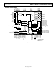

ADuC7019/20/21/22/24/25/26/27/28/29 Data Sheet
Rev. F | Page 10 of 104
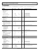
SPECIFICATIONS
AV
DD
= IOV
DD
= 2.7 V to 3.6 V, V
REF
= 2.5 V internal reference, f
CORE
= 41.78 MHz, T
A
= −40°C to +125°C, unless otherwise noted.
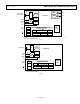
Table 1.
Parameter Min Typ Max Unit Test Conditions/Comments
ADC CHANNEL SPECIFICATIONS Eight acquisition clocks and fADC/2
ADC Power-Up Time 5 μs
DC Accuracy
1, 2
Resolution 12 Bits
Integral Nonlinearity ±0.6 ±1.5 LSB 2.5 V internal reference
±1.0 LSB 1.0 V external reference
Differential Nonlinearity
3, 4
±0.5 +1/−0.9 LSB 2.5 V internal reference
+0.7/−0.6 LSB 1.0 V external reference
DC Code Distribution 1 LSB ADC input is a dc voltage
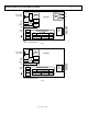
ENDPOINT ERRORS
5
Offset Error ±1 ±2 LSB
Offset Error Match ±1 LSB
Gain Error
±2
±5
LSB
Gain Error Match ±1 LSB
DYNAMIC PERFORMANCE f
IN
= 10 kHz sine wave, f
SAMPLE
= 1 MSPS
Signal-to-Noise Ratio (SNR) 69 dB Includes distortion and noise components
Total Harmonic Distortion (THD) −78 dB
Peak Harmonic or Spurious Noise
(PHSN)
−75 dB
Channel-to-Channel Crosstalk
−80
dB
Measured on adjacent channels
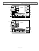
ANALOG INPUT
Input Voltage Ranges
Differential Mode V
CM
6
± V
REF
/2 V
Single-Ended Mode 0 to V
REF
V
Leakage Current ±1 ±6 µA
Input Capacitance 20 pF During ADC acquisition
ON-CHIP VOLTAGE REFERENCE 0.47 µF from V
REF
to AGND
Output Voltage
2.5
V
Accuracy ±5 mV T
A
= 25°C
Reference Temperature Coefficient ±40 ppm/°C
Power Supply Rejection Ratio 75 dB
Output Impedance 70 Ω T
A
= 25°C
Internal V
REF
Power-On Time 1 ms
EXTERNAL REFERENCE INPUT
Input Voltage Range 0.625
AV
DD
V
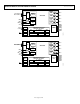
DAC CHANNEL SPECIFICATIONS R
L
= 5 kΩ, C
L
= 100 pF
DC Accuracy
7
Resolution 12 Bits
Relative Accuracy ±2 LSB
Differential Nonlinearity ±1 LSB Guaranteed monotonic
Offset Error
±15
mV
2.5 V internal reference
Gain Error
8
±1 %
Gain Error Mismatch 0.1 % % of full scale on DAC0
ANALOG OUTPUTS
Output Voltage Range_0 0 to DAC
REF
V DAC
REF
range: DACGND to DACV
DD
Output Voltage Range_1 0 to 2.5 V
Output Voltage Range_2 0 to DACV
DD
V
Output Impedance 2 Ω