
Datasheet

ADuC7019/20/21/22/24/25/26/27/28/29 Data Sheet
Rev. F | Page 2 of 104
TABLE OF CONTENTS
Features .............................................................................................. 1
Applications ....................................................................................... 1
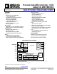
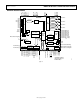
Functional Block Diagram .............................................................. 1
Revision History ............................................................................... 3
General Description ......................................................................... 4
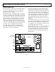
Detailed Block Diagram .............................................................. 9
Specifications ................................................................................... 10
Timing Specifications ................................................................ 13
Absolute Maximum Ratings .......................................................... 20
ESD Caution ................................................................................ 20
Pin Configurations and Function Descriptions ......................... 21
ADuC7019/ADuC7020/ADuC7021/ADuC7022 .................. 21
ADuC7024/ADuC7025 ............................................................. 25
ADuC7026/ADuC7027 ............................................................. 28
ADuC7028 ................................................................................... 31
ADuC7029 ................................................................................... 33
Typical Performance Characteristics ........................................... 35
Terminology .................................................................................... 38
ADC Specifications .................................................................... 38
DAC Specifications..................................................................... 38
Overview of the ARM7TDMI Core ............................................. 39
Thumb Mode (T) ........................................................................ 39
Long Multiply (M) ...................................................................... 39
EmbeddedICE (I) ....................................................................... 39
Exceptions ................................................................................... 39
ARM Registers ............................................................................ 39
Interrupt Latency ........................................................................ 40
Memory Organization ................................................................... 41
Memory Access ........................................................................... 41
Flash/EE Memory ....................................................................... 41
SRAM ........................................................................................... 41
Memory Mapped Registers ....................................................... 41
ADC Circuit Overview .................................................................. 45
Transfer Function ....................................................................... 45
Typical Operation ....................................................................... 46
MMRs Interface .......................................................................... 46
Converter Operation .................................................................. 48
Driving the Analog Inputs ........................................................ 49
Calibration................................................................................... 50
Temperature Sensor ................................................................... 50
Band Gap Reference ................................................................... 50
Nonvolatile Flash/EE Memory ..................................................... 51
Programming .............................................................................. 51
Security ........................................................................................ 52
Flash/EE Control Interface ....................................................... 52
Execution Time from SRAM and Flash/EE ............................ 54
Reset and Remap ........................................................................ 54
Other Analog Peripherals .............................................................. 56
DAC .............................................................................................. 56
Power Supply Monitor ............................................................... 57
Comparator ................................................................................. 57
Oscillator and PLL—Power Control ........................................ 58
Digital Peripherals .......................................................................... 61
3-Phase PWM ............................................................................. 61
Description of the PWM Block ................................................ 62
General-Purpose Input/Output................................................ 67
Serial Port Mux ........................................................................... 70
UART Serial Interface ................................................................ 70
Serial Peripheral Interface ......................................................... 74
I
2
C-Compatible Interfaces ......................................................... 76
Programmable Logic Array (PLA)........................................... 80
Processor Reference Peripherals ................................................... 83
Interrupt System ......................................................................... 83
Timers .......................................................................................... 84
External Memory Interfacing ................................................... 89
Hardware Design Considerations ................................................ 93
Power Supplies ............................................................................ 93
Grounding and Board Layout Recommendations ................. 94
Clock Oscillator .......................................................................... 94
Power-On Reset Operation ....................................................... 95
Typical System Configuration .................................................. 95
Development Tools......................................................................... 96
PC-Based Tools ........................................................................... 96
In-Circuit Serial Downloader ................................................... 96
Outline Dimensions ....................................................................... 97
Ordering Guide ........................................................................ 101