
Inc. Computer Hardware User Manual
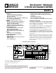

REV. B
–3–
ADuC812
ADuC812BS
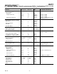
Parameter V
DD
= 5 V V
DD
= 3 V Unit Test Conditions/Comments
ADC CHANNEL SPECIFICATIONS
DC ACCURACY
3, 4
Resolution 12 12 Bits
Integral Nonlinearity ± 1/2 ± 1/2 LSB typ f
SAMPLE
= 100 kHz
± 1.5 LSB max f
SAMPLE
= 100 kHz
± 1.5 ±1.5 LSB typ f
SAMPLE
= 200 kHz
Differential Nonlinearity ± 1 ± 1 LSB typ f
SAMPLE
= 100 kHz. Guaranteed No
Missing Codes at 5 V
CALIBRATED ENDPOINT ERRORS
5, 6
Offset Error ± 5LSB max
± 1 ± 2 LSB typ
Offset Error Match 1 1 LSB typ
Gain Error ± 6LSB max
± 1 ± 2 LSB typ
Gain Error Match 1.5 1.5 LSB typ
USER SYSTEM CALIBRATION
7
Offset Calibration Range ± 5 ±5 % of V
REF
typ
Gain Calibration Range ± 2.5 ±2.5 % of V
REF
typ
DYNAMIC PERFORMANCE f
IN
= 10 kHz Sine Wave
f
SAMPLE
= 100 kHz
Signal-to-Noise Ratio (SNR)
8
70 70 dB typ
Total Harmonic Distortion (THD) –78 –78 dB typ
Peak Harmonic or Spurious Noise –78 –78 dB typ
ANALOG INPUT
Input Voltage Ranges 0 to V
REF
0 to V
REF
Volts
Leakage Current ± 10 µA max
± 1 ± 1 µA typ
Input Capacitance
9
20 20 pF max
TEMPERATURE SENSOR
10
Voltage Output at 25°C 600 600 mV typ Can vary significantly (> ±20%)
Voltage TC –3.0 –3.0 mV/°C typ from device to device
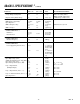
DAC CHANNEL SPECIFICATIONS
DC ACCURACY
11
Resolution 12 12 Bits
Relative Accuracy ± 3 ± 3 LSB typ
Differential Nonlinearity ±0.5 ±1 LSB typ Guaranteed 12-Bit Monotonic
Offset Error ± 60 mV max
± 25 ± 25 mV typ
Full-Scale Error ± 30 mV max
± 10 ± 10 mV typ
Full-Scale Mismatch ± 0.5 ±0.5 % typ % of Full-Scale on DAC1
ANALOG OUTPUTS
Voltage Range_0 0 to V
REF
0 to V
REF
V typ
Voltage Range_1 0 to V
DD
0 to V
DD
V typ
Resistive Load 10 10 kΩ typ
Capacitive Load 100 100 pF typ
Output Impedance 0.5 0.5 Ω typ
I
SINK
50 50 µA typ
SPECIFICATIONS
1, 2
(AV
DD
= DV
DD
= 3.0 V or 5.0 V 10%, REF
IN
/REF
OUT
= 2.5 V Internal Reference, MCLKIN = 11.0592 MHz,
f
SAMPLE
= 200 kHz, DAC V
OUT
Load to AGND; R
L
= 2 k, C
L
= 100 pF. All specifications T
A
= T
MIN
to T
MAX
, unless otherwise noted.)