
Inc. Computer Hardware User Manual

REV. B
ADuC812
–44–
C1+
V+
C1–
C2+
C2–
V–
T2OUT
R2IN
V
CC
GND
T1OUT
R1IN
R1OUT
T1IN
T2IN
R2OUT
ADM202
DV
DD
27
34
33
31
30
29
28
39
38
37
36
35
32
40
47
46
44
43
42
41
52
51
50
49
48
45
DV
DD
1k
DV
DD
1k
2-PIN HEADER FOR
EMULATION ACCESS
(NORMALLY OPEN)
DOWNLOAD/DEBUG
ENABLE JUMPER
(NORMALLY OPEN)
11.0592MHz
DV
DD
1
9-PIN D-SUB
FEMALE
2
3
4
5
6
7
8
9
AV
DD
AV
DD
AGND
C
REF
V
REF
DAC0
DAC1
DV
DD
DGND
PSEN
EA
DGND
DV
DD
XTAL2
XTAL1
RESET
RxD
TxD
DV
DD
DGND
ADM810
V
CC
RST
GND
DVDD
NOT CONNECTED IN THIS EXAMPLE
DV
DD
ADuC812
DAC OUTPUT
51
V
REF
OUTPUT
ADC0
ADC7
ANALOG INPUT
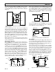
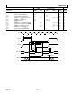
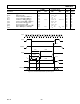
Figure 46. Typical System Configuration
*Application Note uC006 is available at www.analog.com/microconverter
OTHER HARDWARE CONSIDERATIONS
To facilitate in-circuit programming, plus in-circuit debug and
emulation options, users will want to implement some simple
connection points in their hardware that will allow easy access to
download, debug, and emulation modes.
In-Circuit Serial Download Access
Nearly all ADuC812 designs will want to take advantage of the
in-circuit reprogrammability of the chip. This is accomplished by a
connection to the ADuC812’s UART, which requires an external
RS-232 chip for level translation if downloading code from a PC.
Basic configuration of an RS-232 connection is illustrated in
Figure 46 with a simple ADM202-based circuit. If users would
rather not design an RS-232 chip onto a board, refer to the applica-
tion note “uC006–A 4-Wire UART-to-PC Interface”* for a
simple (and zero-cost-per-board) method of gaining in-circuit
serial download access to the ADuC812.
In addition to the basic UART connections, users will also need
a way to trigger the chip into download mode. This is accom-
plished via a 1 kΩ pull-down resistor that can be jumpered onto
the PSEN pin, as shown in Figure 46. To get the ADuC812
into download mode, simply connect this jumper and power-
cycle the device (or manually reset the device, if a manual reset
button is available) and it will be ready to receive a new program
serially. With the jumper removed, the device will come up in
normal mode (and run the program) whenever power is cycled
or RESET is toggled.
Note that PSEN is normally an output (as described in the
External Memory Interface section) and it is sampled as an
input only on the falling edge of RESET (i.e., at power-up or
upon an external manual reset). Note also that if any external
circuitry unintentionally pulls PSEN low during power-up or
reset events, it could cause the chip to enter download mode and
therefore fail to begin user code execution as it should. To pre-
vent this, ensure that no external signals are capable of pulling
the PSEN pin low, except for the external PSEN jumper itself.
Embedded Serial Port Debugger
From a hardware perspective, entry to serial port debug mode is
identical to the serial download entry sequence described above.
In fact, both serial download and serial port debug modes can be
thought of as essentially one mode of operation used in two
different ways.