
Inc. Computer Hardware User Manual

REV. B
ADuC812
–6–
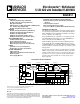
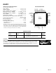
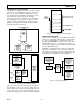
PIN CONFIGURATION
52 51 50 49 48 43 42 41 4047 46 45 44
14 15 16 17 18 19 20 21 22 23 24 25 26
1
2
3
4
5
6
7
8
9
10
13
12
11
39
38
37
36
35
34
33
32
31
30
29
28
27
PIN 1
IDENTIFIER
TOP VIEW
(Not to Scale)
P0.7/AD7
P0.6/AD6
P0.5/AD5
P0.4/AD4
DV
DD
DGND
P0.3/AD3
P0.2/AD2
P0.1/AD1
P0.0/AD0
ALE
PSEN
EA
P1.0/ADC0/T2
P1.1/ADC1/T2EX
P1.2/ADC2
P1.3/ADC3
AV
DD
AGND
C
REF
V
REF
DAC0
DAC1
P1.4/ADC4
P1.5/ADC5/SS
P1.6/ADC6
P2.7/A15/A23
P2.6/A14/A22
P2.5/A13/A21
P2.4/A12/A20
DGND
DV
DD
XTAL2
XTAL1
P2.3/A11/A19
P2.2/A10/A18
P2.1/A9/A17
P2.0/A8/A16
SDATA/MOSI
P1.7/ADC7
RESET
P3.0/RxD
P3.1/TxD
P3.2/INT0
P3.3/INT1/MISO
DV
DD
DGND
P3.4/T0
P3.5/T1/CONVST
P3.7/RD
SCLOCK
P3.6/WR
ADuC812
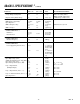
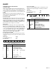
ORDERING GUIDE
Temperature Package Package
Model Range Description Option
ADuC812BS –40°C to +85°C 52-Lead Plastic Quad Flatpack S-52
Eval-ADuC812QS QuickStart Development System
CAUTION
ESD (electrostatic discharge) sensitive device. Electrostatic charges as high as 4000 V readily
accumulate on the human body and test equipment and can discharge without detection. Although
the ADuC812 features proprietary ESD protection circuitry, permanent damage may occur on
devices subjected to high-energy electrostatic discharges. Therefore, proper ESD precautions are
recommended to avoid performance degradation or loss of functionality.
WARNING!
ESD SENSITIVE DEVICE
ABSOLUTE MAXIMUM RATINGS*
(T
A
= 25°C unless otherwise noted)
AV
DD
to DV
DD
. . . . . . . . . . . . . . . . . . . . . . –0.3 V to +0.3 V
AGND to DGND . . . . . . . . . . . . . . . . . . . . –0.3 V to +0.3 V
DV
DD
to DGND, AV
DD
to AGND . . . . . . . . . –0.3 V to +7 V
Digital Input Voltage to DGND . . . . . –0.3 V, DV
DD
+ 0.3 V
Digital Output Voltage to DGND . . . . –0.3 V, DV
DD
+ 0.3 V
V
REF
to AGND . . . . . . . . . . . . . . . . . . –0.3 V, AV
DD
+ 0.3 V
Analog Inputs to AGND . . . . . . . . . . . –0.3 V, AV
DD
+ 0.3 V
Operating Temperature Range Industrial (B Version)
. . . . . . . . . . . . . . . . . . . . . . . . . . . . . . . . . . –40°C to +85°C
Storage Temperature Range . . . . . . . . . . . . –65°C to +150°C
Junction Temperature . . . . . . . . . . . . . . . . . . . . . . . . . 150°C
θ
JA
Thermal Impedance . . . . . . . . . . . . . . . . . . . . . . . 90°C/W
Lead Temperature, Soldering
Vapor Phase (60 sec) . . . . . . . . . . . . . . . . . . . . . . . . 215°C
Infrared (15 sec) . . . . . . . . . . . . . . . . . . . . . . . . . . . 220°C
*Stresses above those listed under Absolute Maximum Ratings may cause perma-
nent damage to the device. This is a stress rating only; functional operation of the
device at these or any other conditions above those listed in the operational
sections of this specification is not implied. Exposure to absolute maximum rating
conditions for extended periods may affect device reliability.