
Datasheet
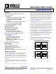


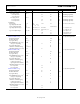
Table Of Contents
- Features
- Applications
- General Description
- Functional Block Diagrams
- Revision History
- Specifications
- Electrical Characteristics—5 V, 105 C Operation
- Electrical Characteristics—3 V, 105 C Operation
- Electrical Characteristics—Mixed 5 V/3 V or 3 V/5 V, 105 C Operation
- Electrical Characteristics—5 V, 125 C Operation
- Electrical Characteristics—3 V, 125 C Operation
- Electrical Characteristics—Mixed 5 V/3 V, 125 C Operation
- Electrical Characteristics—Mixed 3 V/5 V, 125 C Operation
- Package Characteristics
- Regulatory Information
- Insulation and Safety-Related Specifications
- DIN V VDE V 0884-10 (VDE V 0884-10): 2006-12 Insulation Characteristics
- Recommended Operating Conditions
- Absolute Maximum Ratings
- Pin Configurations and Function Descriptions
- Typical Performance Characteristics
- Applications Information
- Outline Dimensions

Data Sheet ADuM1200/ADuM1201
Rev. K | Page 7 of 28
Parameter Symbol Min Typ Max Unit Test Conditions/Comments
ADuM1200/ADuM1201BR C
L
= 15 pF, CMOS signal levels
Minimum Pulse Width
2
PW 100 ns
Maximum Data Rate
3
10 Mbps
Propagation Delay
4
t
PHL
, t
PLH
20 60 ns
Pulse Width Distortion, |t
PLH
− t
PHL
|
4
PWD 3 ns
Change vs. Temperature 5 ps/°C
Propagation Delay Skew
5
t
PSK
22 ns
Channel-to-Channel Matching
Codirectional Channels
6
t
PSKCD
3 ns
Opposing Directional Channels
6
t
PSKOD
22 ns
Output Rise/Fall Time (10% to 90%) t
R
/t
F
3.0 ns
ADuM1200/ADuM1201CR
Minimum Pulse Width
2
PW 20 40 ns
Maximum Data Rate
3
25 50 Mbps
Propagation Delay
4
t
PHL
, t
PLH
20 55 ns
Pulse Width Distortion, |t
PLH
− t
PHL
|
4
PWD 3 ns
Change vs. Temperature 5 ps/°C
Propagation Delay Skew
5
t
PSK
16 ns
Channel-to-Channel Matching
Codirectional Channels
6
t
PSKCD
3 ns
Opposing Directional Channels
6
t
PSKOD
16 ns
Output Rise/Fall Time (10% to 90%)
t
R
/t
F
3.0
ns
For All Models
Common-Mode Transient Immunity
Logic High Output
7
|CM
H
| 25 35 kV/µs
V
Ix
= V
DD1
or V
DD2
, V
CM
= 1000 V,
transient magnitude = 800 V
Logic Low Output
7
|CM
L
| 25 35 kV/µs
V
Ix
= 0 V, V
CM
= 1000 V,
transient magnitude = 800 V
Refresh Rate f
r
1.1 Mbps
Dynamic Supply Current per Channel
8
Input I
DDI (D)
0.10
mA/
Mbps
Output I
DDO (D)
0.03
mA/
Mbps
1
The supply current values are for both channels combined when running at identical data rates. Output supply current values are specified with no output load
present. The supply current associated with an individual channel operating at a given data rate can be calculated as described in the Power Consumption section. See
Figure 6 through Figure 8 for information on per-channel supply current as a function of data rate for unloaded and loaded conditions. See Figure 9 through Figure 11
for total V
DD1
and V
DD2
supply currents as a function of data rate for ADuM1200 and ADuM1201 channel configurations.
2
The minimum pulse width is the shortest pulse width at which the specified pulse width distortion is guaranteed.
3
The maximum data rate is the fastest data rate at which the specified pulse width distortion is guaranteed.
4
t
PHL
propagation delay is measured from the 50% level of the falling edge of the V
Ix
signal to the 50% level of the falling edge of the V
Ox
signal. t
PLH
propagation delay is
measured from the 50% level of the rising edge of the V
Ix
signal to the 50% level of the rising edge of the V
Ox
signal.
5
t
PSK
is the magnitude of the worst-case difference in t
PHL
and/or t
PLH
that is measured between units at the same operating temperature, supply voltages, and output
load within the recommended operating conditions.
6
Codirectional channel-to-channel matching is the absolute value of the difference in propagation delays between any two channels with inputs on the same side of
the isolation barrier. Opposing directional channel-to-channel matching is the absolute value of the difference in propagation delays between any two channels with
inputs on opposing sides of the isolation barrier.
7
CM
H
is the maximum common-mode voltage slew rate that can be sustained while maintaining V
O
> 0.8 V
DD2
. CM
L
is the maximum common-mode voltage slew rate
that can be sustained while maintaining V
O
< 0.8 V. The common-mode voltage slew rates apply to both rising and falling common-mode voltage edges. The transient
magnitude is the range over which the common mode is slewed.
8
Dynamic supply current is the incremental amount of supply current required for a 1 Mbps increase in the signal data rate. See Figure 6 through Figure 8 for
information on per-channel supply current as a function of data rate for unloaded and loaded conditions. See the Power Consumption section for guidance on
calculating per-channel supply current for a given data rate.