
Datasheet


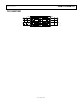
Table Of Contents

ADuM1250/ADuM1251 Data Sheet
Rev. I | Page 10 of 16
APPLICATIONS INFORMATION
FUNCTIONAL DESCRIPTION
The ADuM1250/ADuM1251 interface on each side to a
bidirectional I
2
C signal. Internally, the I
2
C interface is split
into two unidirectional channels communicating in opposing
directions via a dedicated iCoupler isolation channel for each.
One channel (the bottom channel of each channel pair shown
in Figure 6) senses the voltage state of the Side 1 I
2
C pin and
transmits its state to its respective Side 2 I
2
C pin.
Both the Side 1 and the Side 2 I
2
C pins are designed to interface
to an I
2
C bus operating in the 3.0 V to 5.5 V range. A logic low
on either pin causes the opposite pin to be pulled low enough to
comply with the logic low threshold requirements of other I
2
C
devices on the bus. Avoidance of I
2
C bus contention is ensured
by an input low threshold at SDA
1
or SCL
1
guaranteed to be at
least 50 mV less than the output low signal at the same pin.
This prevents an output logic low at Side 1 being transmitted
back to Side 2 and pulling down the I
2
C bus.
Because the Side 2 logic levels/thresholds are standard I
2
C values,
multiple ADuM1250/ADuM1251 devices connected to a bus by
their Side 2 pins can communicate with each other and with other
I
2
C compatible devices. A distinction is made between I
2
C compat-
ibility and I
2
C compliance. I
2
C compatibility refers to situations in
which the logic levels of a component do not necessarily meet the
requirements of the I
2
C specification but still allow the component
to communicate with an I
2
C compliant device. I
2
C compliance
refers to situations in which the logic levels of a component meet
the requirements of the I
2
C specification.
However, because the Side 1 pin has a modified output level/
input threshold, this side of the ADuM1250/ADuM1251 can
communicate only with devices that conform to the I
2
C stan-
dard. In other words, Side 2 of the ADuM1250/ADuM1251 is
I
2
C compliant, whereas Side 1 is only I
2
C compatible.
The output logic low levels are independent of the V
DD1
and
V
DD2
voltages. The input logic low threshold at Side 1 is also
independent of V
DD1
. However, the input logic low threshold at
Side 2 is designed to be at 0.3 V
DD2
, consistent with I
2
C require-
ments. The Side 1 and Side 2 pins have open-collector outputs
whose high levels are set via pull-up resistors to their respective
supply voltages.
ENCODE DECODE
DECODE ENCODE
ENCODE DECODE
DECODE ENCODEV
DD1
SDA
1
SCL
1
V
DD2
SDA
2
SCL
2
C
L
GND
2
1
2
3
8
7
6
5
GND
1
4
C
L
R2 R2
0
6113-006
Figure 6. ADuM1250 Block Diagram
STARTUP
Both the V
DD1
and V
DD2
supplies have an undervoltage lockout
feature to prevent the signal channels from operating unless
certain criteria are met. This feature prevents input logic low
signals from pulling down the I
2
C bus inadvertently during
power-up/power-down.
For the signal channels to be enabled, the following two criteria
must be met:
Both supplies must be at least 2.5 V.
At least 40 s must elapse after both supplies exceed the
internal startup threshold of 2.0 V.
Until both criteria are met for both supplies, the ADuM1250/
ADuM1251 outputs are pulled high, ensuring a startup that
avoids any disturbances on the bus. Figure 7 and Figure 8 illustrate
the supply conditions for fast and slow input supply slew rates.
MINIMUM RECOMMENDED
OPERATING SUPPLY, 3.0V
MINIMUM VALID SUPPLY, 2.5V
INTERNAL START-UP
THRESHOLD, 2.0V
40µs
SUPPLY VALID
06113-007
Figure 7. Start-Up Condition, Supply Slew Rate > 12.5 V/ms
40µs
SUPPLY VALID
MINIMUM RECOMMENDED
OPERATING SUPPLY, 3.0V
MINIMUM VALID SUPPLY, 2.5V
INTERNAL START-UP
THRESHOLD, 2.0V
06113-008
Figure 8. Start-Up Condition, Supply Slew Rate < 12.5 V/ms