
Datasheet


Data Sheet ADuM1250/ADuM1251
Rev. H | Page 11 of 16
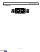
TYPICAL APPLICATION DIAGRAM
Figure 9 shows a typical application circuit including the pull-up
resistors required for both Side 1 and Side 2 buses. Bypass capaci-
tors with values from 0.01 μF to 0.1 μF are required between V
DD1
and GND
1
and between V
DD2
and GND
2
. The 200 Ω resistor shown
in Figure 9 is required for latch-up immunity if the ambient
temperature can be between 105°C and 125°C.
V
DD1
GND
1
SDA
1
GND
2
V
DD2
SDA
2
ADuM1250
SCL
1
SCL
2
I
2
C BUS
1
2
3
4
8
7
6
5
06113-009
OPTIONAL
200Ω
Figure 9. Typical Isolated I
2
C Interface Using the ADuM1250
CAPACITIVE LOAD AT LOW SPEEDS
The ADuM1250/ADuM1251 are designed for operation at
speeds up to 1 Mbps. Due to the limited current available on
Side 1, operation at 1 Mbps limits the capacitance that can be
driven at the minimum pull-up value to 40 pF.
Most applications operate at 100 kbps in standard mode or
400 kbps in fast mode. At these lower operating speeds, the
limitation on the load capacitance can be significantly relaxed.
Table 11 shows the maximum capacitance at minimum pull-up
values for standard and fast operating modes. If larger values for
the pull up resistor are used, the maximum supported capacitance
must be scaled down proportionately so that the rise time does
not increase beyond the values required by the standard.
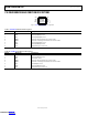
Table 11. Side 1 Maximum Load Conditions
Maximum Capacitive Load for Side 1
Mode V
DD1
Data Rate (kbps) t
r
(ns) t
f
(ns) R
1
(Ω) C
L1
(pF)
Standard 5 100 1000 187 1600 484
Fast 5 400 300 172 1600 120
Standard 3.3 100 1000 270 1000 771
Fast 3.3 400 300 235 1000 188
Downloaded from Arrow.com.Downloaded from Arrow.com.Downloaded from Arrow.com.Downloaded from Arrow.com.Downloaded from Arrow.com.Downloaded from Arrow.com.Downloaded from Arrow.com.Downloaded from Arrow.com.Downloaded from Arrow.com.Downloaded from Arrow.com.Downloaded from Arrow.com.