
Datasheet


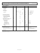
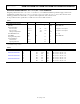
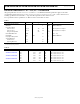


Table Of Contents
- Features
- Applications
- General Description
- Functional Block Diagrams
- Revision History
- Specifications
- Electrical Characteristics—3.3 V Operation
- Electrical Characteristics—2.5 V Operation
- Electrical Characteristics—VDD1 = 3.3 V, VDD2 = 2.5 V Operation
- Electrical Characteristics—VDD1 = 2.5 V, VDD2 = 3.3 V Operation
- Package Characteristics
- Regulatory Information
- Insulation and Safety Related Specifications
- DIN V VDE V 0884-10 (VDE V 0884-10):2006-12 Insulation Characteristics
- Intrinsic Safety
- Absolute Maximum Ratings
- Pin Configurations and Function Descriptions
- Typical Performance Characteristics
- Applications Information
- Outline Dimensions

ADuM1440/ADuM1441/ADuM1442/ADuM1445/ADuM1446/ADuM1447 Data Sheet
Rev. E | Page 10 of 25
INSULATION AND SAFETY RELATED SPECIFICATIONS
Table 13.
Parameter Symbol Value Unit Test Conditions/Comments
Rated Dielectric Insulation Voltage (RQ-16)
2500
V rms
1-minute duration
Rated Dielectric Insulation Voltage (RS-20) 3750 V rms 1-minute duration
Minimum External Tracking and Air Gap, RQ-16 (Creepage
and Clearance)
L(I02) 3.1 mm min Measured from input terminals to output
terminals, shortest distance path along
package body
Minimum Clearance in the Plane of the Printed Circuit
Board, RQ-16 (PCB Clearance)
L(I01) 3.8 mm min Measured from input terminals to output
terminals, shortest distance through air, line
of sight, in the PCB mounting plane
Minimum External Tracking and Air Gap, RS-20 (Creepage
and Clearance)
L(I01) 5.1 mm min Measured from input terminals to output
terminals, shortest distance path along
package body
Minimum Clearance in the Plane of the Printed Circuit
Board, RS-20 (PCB Clearance)
L(I02) 5.1 mm min Measured from input terminals to output
terminals, shortest distance through air, line
of sight, in the PCB mounting plane
Minimum Internal Gap (Internal Clearance) 0.017 mm min Insulation distance through insulation
Tracking Resistance (Comparative Tracking Index) CTI >400 V DIN IEC 112/VDE 0303 Part 1
Isolation Group II Material Group (DIN VDE 0110, 1/89, Table 1)
DIN V VDE V 0884-10 (VDE V 0884-10):2006-12 INSULATION CHARACTERISTICS
These isolators are suitable for reinforced electrical isolation within the safety limit data only. Maintenance of the safety data is ensured by
protective circuits. The asterisk (*) marked on packages denotes DIN V VDE V 0884-10 approval.
Table 14. 16-Lead QSOP (RQ-16)
Description Test Conditions/Comments Symbol Characteristic Unit
Installation Classification per DIN VDE 0110
For Rated Mains Voltage ≤ 150 V rms I to IV
For Rated Mains Voltage ≤ 300 V rms I to III
For Rated Mains Voltage ≤ 400 V rms I to II
Climatic Classification 40/105/21
Pollution Degree per DIN VDE 0110, Table 1 2
Maximum Working Insulation Voltage V
IORM
565 V
PEAK
Input-to-Output Test Voltage, Method b1 V
IORM
× 1.875 = V
pd(m)
, 100% production test,
t
ini
= t
m
= 1 sec, partial discharge < 5 pC
V
pd(m)
1059 V
PEAK
Input-to-Output Test Voltage, Method a
After Environmental Tests Subgroup 1 V
IORM
× 1.5 = V
pd(m)
, t
ini
= 60 sec, t
m
= 10 sec,
partial discharge < 5 pC
V
pd(m)
847 V
PEAK
After Input and/or Safety Test Subgroup 2
and Subgroup 3
V
IORM
× 1.2 = V
pd(m)
, t
ini
= 60 sec, t
m
= 10 sec,
partial discharge < 5 pC
V
pd(m)
678
V
PEAK
Highest Allowable Overvoltage V
IOTM
4000 V
PEAK
Surge Isolation Voltage V
PEAK
= 10 kV, 1.2 µs rise time, 50 µs, 50% fall time V
IOSM
6250 V
PEAK
Safety Limiting Values Maximum value allowed in the event of a failure
(see Figure 4)
Case Temperature T
S
150 °C
Total Power Dissipation at 25°C I
S1
1.64 W
Insulation Resistance at T
S
V
IO
= 500 V R
S
>10
9
Ω