
Datasheet
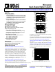


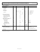


Table Of Contents
- Features
- Applications
- General Description
- Functional Block Diagrams
- Revision History
- Specifications
- Electrical Characteristics—3.3 V Operation
- Electrical Characteristics—2.5 V Operation
- Electrical Characteristics—VDD1 = 3.3 V, VDD2 = 2.5 V Operation
- Electrical Characteristics—VDD1 = 2.5 V, VDD2 = 3.3 V Operation
- Package Characteristics
- Regulatory Information
- Insulation and Safety Related Specifications
- DIN V VDE V 0884-10 (VDE V 0884-10):2006-12 Insulation Characteristics
- Intrinsic Safety
- Absolute Maximum Ratings
- Pin Configurations and Function Descriptions
- Typical Performance Characteristics
- Applications Information
- Outline Dimensions

ADuM1440/ADuM1441/ADuM1442/ADuM1445/ADuM1446/ADuM1447 Data Sheet
Rev. E | Page 2 of 25
TABLE OF CONTENTS
Features .............................................................................................. 1
Applications ....................................................................................... 1
General Description ......................................................................... 1
Functional Block Diagrams ............................................................. 1
Revision History ............................................................................... 2
Specifications ..................................................................................... 3
Electrical Characteristics—3.3 V Operation ............................ 3
Electrical Characteristics—2.5 V Operation ............................ 5
Electrical Characteristics—V
DD1
= 3.3 V, V
DD2
= 2.5 V
Operation ....................................................................................... 7
Electrical Characteristics—V
DD1
= 2.5 V, V
DD2
= 3.3 V
Operation ....................................................................................... 8
Package Characteristics ............................................................... 9
Regulatory Information ............................................................... 9
Insulation and Safety Related Specifications .......................... 10
DIN V VDE V 0884-10 (VDE V 0884-10):2006-12 Insulation
Characteristics ............................................................................ 10
Intrinsic Safety ............................................................................ 11
Absolute Maximum Ratings ......................................................... 13
ESD Caution................................................................................ 13
Pin Configurations and Function Descriptions ......................... 14
Typical Performance Characteristics ........................................... 17
Applications Information .............................................................. 20
PCB Layout ................................................................................. 20
Propagation Delay-Related Parameters ................................... 20
DC Correctness ............................................................................ 20
Magnetic Field Immunity ............................................................. 21
Power Consumption .................................................................. 22
Insulation Lifetime ..................................................................... 22
Outline Dimensions ....................................................................... 24
Ordering Guide .......................................................................... 25
REVISION HISTORY
1/2017—Rev. D to Rev. E
Changes to Features Section............................................................ 1
Changes to Table 12 .......................................................................... 9
Added Intrinsic Safety Section, Table 16; Renumbered Sequentially,
and Table 17 ..................................................................................... 11
4/2015—Rev. C to Rev. D
Change to General Description Section ........................................ 1
4/2015—Rev. B to Rev. C
Changes to Regulatory Information Section ................................ 9
3/2015—Rev. A to Rev. B
Changes to Features Section and Figure 3 ..................................... 1
Changes to Table 12 .......................................................................... 9
Changes to Table 13 and Table 14 ................................................ 10
Updated Outline Dimensions ....................................................... 23
Changes to Ordering Guide .......................................................... 24
3/2014—Rev. 0 to Rev. A
Added SSOP Package ......................................................... Universal
Changes to Features Section, Added Figure 2,
Renumbered Sequentially ................................................................ 1
Changes to Output Voltage Logic High Parameter, Table 3 ........ 4
Added Table 15, Renumbered Sequentially; Changes to
Figure 4 ............................................................................................ 11
Change to Supply Voltages (V
DD1
, V
DD2
) Parameter, Table 17 ........ 12
Added Figure 6; Changes to Table 20 .......................................... 13
Added Figure 8; Changes to Table 21 .......................................... 14
Added Figure 10, Changes to Table 22 ........................................ 15
Added Figure 30 ............................................................................. 19
Changes to Power Consumption Section; Added Table 23 ...... 21
Added Figure 27 ............................................................................. 23
Changes to Ordering Guide .......................................................... 24
10/2013—Revision 0: Initial Version