
Datasheet
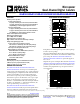


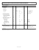
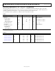


Table Of Contents
- Features
- Applications
- General Description
- Functional Block Diagrams
- Revision History
- Specifications
- Electrical Characteristics—3.3 V Operation
- Electrical Characteristics—2.5 V Operation
- Electrical Characteristics—VDD1 = 3.3 V, VDD2 = 2.5 V Operation
- Electrical Characteristics—VDD1 = 2.5 V, VDD2 = 3.3 V Operation
- Package Characteristics
- Regulatory Information
- Insulation and Safety Related Specifications
- DIN V VDE V 0884-10 (VDE V 0884-10):2006-12 Insulation Characteristics
- Intrinsic Safety
- Absolute Maximum Ratings
- Pin Configurations and Function Descriptions
- Typical Performance Characteristics
- Applications Information
- Outline Dimensions

ADuM1440/ADuM1441/ADuM1442/ADuM1445/ADuM1446/ADuM1447 Data Sheet
Rev. E | Page 4 of 25
Table 3. For All Models
Parameter Symbol Min Typ Max Unit Test Conditions/Comments
DC SPECIFICATIONS
Input Threshold
Logic High V
IH
0.7 V
DDx
1
V
Logic Low V
IL
0.3 V
DDx
1
V
Output Voltages
Logic High V
OH
V
DDx
1
− 0.1 3.3 V I
OUTx
= −20 µA, V
Ix
= V
IxH
V
DDx
1
− 0.4 3.1 V I
OUTx
= −4 mA, V
Ix
= V
IxH
Logic Low V
OL
0.0 0.1 V I
OUTx
= 20 µA, V
Ix
= V
IxL
0.2 0.4 V I
OUTx
= 4 mA, V
Ix
= V
IxL
Input Current per Channel I
I
−1 +0.01 +1 µA 0 V ≤ V
Ix
≤ V
DDx
1
Input Switching Thresholds
Positive Threshold Voltage V
T+
1.8 V
Negative Going Threshold V
T−
1.2 V
Input Hysteresis ΔV
T
0.6 V
Undervoltage Lockout, V
DD1
or V
DD2
UVLO 1.5 V
Supply Current per Channel
Quiescent Current
Input Supply I
DDI (Q)
4.8 10 µA EN
X
low
Output Supply I
DDO (Q)
0.8 3.3 µA EN
X
low
Input (Refresh Off ) I
DDI (Q)
0.12 µA EN
X
high
Output (Refresh Off)
I
DDO (Q)
0.13
µA
EN
X
high
Dynamic Supply Current
Input I
DDI (D)
88 µA/Mbps
Output I
DDO (D)
60 µA/Mbps
AC SPECIFICATIONS
Output Rise Time/Fall Time t
R
/t
F
2 ns 10% to 90%
Common-Mode Transient Immunity
2
|CM| 25 40 kV/µs V
Ix
= V
DDx
1
, V
CM
= 1000 V,
transient magnitude = 800 V
Refresh Rate f
r
14 kbps
1
V
DDx
= V
DD1
or V
DD2
.
2
|CM| is the maximum common-mode voltage slew rate that can be sustained while maintaining V
OUT
> 0.8 V
DDx
. The common-mode voltage slew rates apply to both rising and
falling common-mode voltage edges.