
Datasheet
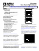


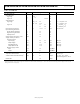
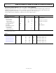
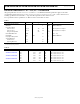


Table Of Contents
- Features
- Applications
- General Description
- Functional Block Diagrams
- Revision History
- Specifications
- Electrical Characteristics—3.3 V Operation
- Electrical Characteristics—2.5 V Operation
- Electrical Characteristics—VDD1 = 3.3 V, VDD2 = 2.5 V Operation
- Electrical Characteristics—VDD1 = 2.5 V, VDD2 = 3.3 V Operation
- Package Characteristics
- Regulatory Information
- Insulation and Safety Related Specifications
- DIN V VDE V 0884-10 (VDE V 0884-10):2006-12 Insulation Characteristics
- Intrinsic Safety
- Absolute Maximum Ratings
- Pin Configurations and Function Descriptions
- Typical Performance Characteristics
- Applications Information
- Outline Dimensions

Data Sheet ADuM1440/ADuM1441/ADuM1442/ADuM1445/ADuM1446/ADuM1447
Rev. E | Page 5 of 25
ELECTRICAL CHARACTERISTICS—2.5 V OPERATION
All typical specifications are at T
A
= 25°C, V
DD1
= V
DD2
= 2.5 V. Minimum/maximum specifications apply over the entire recommended
operating range of 2.25 V ≤ V
DD1
≤ 2.75 V, 2.25 V ≤ V
DD2
≤ 2.75 V, and −40°C ≤ T
A
≤ +125°C, unless otherwise noted. Switching
specifications are tested with C
L
= 15 pF, and CMOS signal levels, unless otherwise noted.
Table 4.
Parameter Symbol Min Typ Max Unit Test Conditions/Comments
SWITCHING SPECIFICATIONS
Data Rate 2 Mbps Within PWD limit
Propagation Delay t
PHL
, t
PLH
112 180 ns 50% input to 50% output
Change vs. Temperature 280 ps/°C
Pulse-Width Distortion PWD 12 ns |t
PLH
− t
PHL
|
Minimum Pulse Width PW 500 ns Within PWD limit
Propagation Delay Skew
1
t
PSK
10 ns
Channel Matching
Codirectional t
PSKCD
10 ns
Opposing Direction
t
PSKOD
30
ns
1
t
PSK
is the magnitude of the worst-case difference in t
PHL
or t
PLH
that is measured between units at the same operating temperature, supply voltages, and output load within the
recommended operating conditions.
Table 5.
Parameter Symbol Min Typ Max Unit Test Conditions/Comments
SUPPLY CURRENT
2 Mbps, no load
ADuM1440/ADuM1445 I
DD1
623 800 µA EN
X
= 0 V, V
IH
= V
DD
, V
IL
= 0 V
I
DD2
337 500 µA EN
X
= 0 V, V
IH
= V
DD
, V
IL
= 0 V
ADuM1441/ADuM1446 I
DD1
552 750 µA EN
X
= 0 V, V
IH
= V
DD
, V
IL
= 0 V
I
DD2
409 750 µA EN
X
= 0 V, V
IH
= V
DD
, V
IL
= 0 V
ADuM1442/ADuM1447 I
DD1
480 750 µA EN
X
= 0 V, V
IH
= V
DD
, V
IL
= 0 V
I
DD2
480 750 µA EN
X
= 0 V, V
IH
= V
DD
, V
IL
= 0 V