
Datasheet


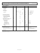
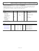
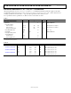


Table Of Contents
- Features
- Applications
- General Description
- Functional Block Diagrams
- Revision History
- Specifications
- Electrical Characteristics—3.3 V Operation
- Electrical Characteristics—2.5 V Operation
- Electrical Characteristics—VDD1 = 3.3 V, VDD2 = 2.5 V Operation
- Electrical Characteristics—VDD1 = 2.5 V, VDD2 = 3.3 V Operation
- Package Characteristics
- Regulatory Information
- Insulation and Safety Related Specifications
- DIN V VDE V 0884-10 (VDE V 0884-10):2006-12 Insulation Characteristics
- Intrinsic Safety
- Absolute Maximum Ratings
- Pin Configurations and Function Descriptions
- Typical Performance Characteristics
- Applications Information
- Outline Dimensions

Data Sheet ADuM1440/ADuM1441/ADuM1442/ADuM1445/ADuM1446/ADuM1447
Rev. E | Page 9 of 25
PACKAGE CHARACTERISTICS
Table 11.
Parameter Symbol Min Typ Max Unit Test Conditions/Comments
Resistance (Input-to-Output)
1
R
I-O
10
13
Ω
Capacitance (Input-to-Output)
1
C
I-O
2 pF f = 1 MHz
Input Capacitance
2
C
I
4.0 pF
IC Junction-to-Ambient Thermal
Resistance (QSOP)
θ
JA
76 °C/W Thermocouple located at center of package underside
IC Junction-to-Ambient Thermal
Resistance (SSOP)
θ
JA
50.5 °C/W Thermocouple located at center of package underside
1
The device is considered a 2-terminal device: Pin 1 through Pin 8 are shorted together, and Pin 9 through Pin 16 are shorted together.
2
Input capacitance is from any input data pin to ground.
REGULATORY INFORMATION
See Table 20 and the Insulation Lifetime section for the recommended maximum working voltages for specific cross-isolation waveforms
and insulation levels.
Table 12. Safety Certifications
UL CSA VDE CSA/Sira
Recognized Under UL
1577 Component
Recognition Program
1
Approved under CSA
Component Acceptance
Notice 5A
Certified according to
DIN V VDE V 0884-10
(VDE V 0884-10):2006-12
2
Certified for use in intrinsic
safety (IS) to IS applications
under ATEX and IECEx
Single Protection CSA 60950-1-07+A1+A2 and
IEC 60950-1 second edition
+A1+A2
QSOP package:
reinforced insulation,
565 V
PEAK
QSOP package
ATEX: EN 60079-0:2012+A11:2013
and EN 60079-11:2012
2500 V RMS Isolation
Voltage (RQ-16 Only)
QSOP package: basic
insulation, 310 V rms
maximum working voltage
SSOP package:
reinforced insulation,
849 V
PEAK
SSOP package
IECEx: IEC 60079-0:2011 Edition 6
and IEC 60079-11:2011 Edition 6
3750 V RMS Isolation
Voltage (RS-20 Only)
SSOP package: basic insulation
at 510 V rms (721 V
PEAK
)
maximum working voltage and
IEC 60601-1 Edition 3.1 250 V
(1 means of patient protection
(MOPP)); reinforced insulation at
255 V rms (360 V
PEAK
) maximum
working voltage
II 1G Ex ia IIC Ga
File E214100 File 205078 File 2471900-4880-0001 File 70013932
1
In accordance with UL 1577, each ADuM1440/ADuM1441/ADuM1442/ADuM1445/ADuM1446/ADuM1447 is proof tested by applying an insulation test voltage and
measuring leakage during final production testing. QSOP package devices are tested at ≥3000 V rms for 1 sec with a current leakage detection limit = 5 μA. SSOP
package devices are tested at ≥4500 V rms for 1 sec with a current leakage detection limit = 10 μA.
2
In accordance with DIN V VDE V 0884-10, each ADuM1440/ADuM1441/ADuM1442/ADuM1445/ADuM1446/ADuM1447 is proof tested by applying an insulation test
voltage ≥1059 V
PEAK
for 1 second (partial discharge detection limit = 5 pC). The asterisk (*) marked on the component designates DIN V VDE V 0884-10 approval.