
Datasheet
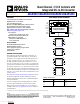


ADuM5401/ADuM5402/ADuM5403/ADuM5404 Data Sheet
Rev. D | Page 8 of 28
ELECTRICAL CHARACTERISTICS—5 V PRIMARY INPUT SUPPLY/3.3 V SECONDARY ISOLATED SUPPLY
Typical specifications are at T
A
= 25°C, V
DD1
= 5.0 V, V
ISO
= 3.3 V, V
SEL
= GND
ISO
. Minimum/maximum specifications apply over the entire
recommended operation range which is 4.5 V ≤ V
DD1
≤ 5.5 V, 3.0 V ≤ V
ISO
≤ 3.6 V; and −40°C ≤ T
A
≤ +105°C, unless otherwise noted.
Switching specifications are tested with C
L
= 15 pF and CMOS signal levels, unless otherwise noted.
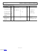
Table 10. DC-to-DC Converter Static Specifications
Parameter Symbol Min Typ Max Unit Test Conditions/Comments
DC-TO-DC CONVERTER SUPPLY
Setpoint V
ISO
3.0 3.3 3.6 V I
ISO
= 0 mA
Line Regulation V
ISO (LINE)
1 mV/V I
ISO
= 50 mA, V
DD1
= 3.0 V to 3.6 V
Load Regulation V
ISO (LOAD)
1 5 % I
ISO
= 6 mA to 54 mA
Output Ripple V
ISO (RIP)
50 mV p-p 20 MHz bandwidth, C
BO
= 0.1 μF||10 μF, I
ISO
= 90 mA
Output Noise V
ISO (NOISE)
130 mV p-p C
BO
= 0.1 μF||10 μF, I
ISO
= 90 mA
Switching Frequency f
OSC
180 MHz
PWM Frequency f
PWM
625 kHz
Output Supply Current I
ISO (MAX)
100 mA V
ISO
> 3 V
Efficiency at I
ISO (MAX)
30 % I
ISO
= 90 mA
I
DD1
, No V
ISO
Load I
DD1 (Q)
14 20 mA
I
DD1
, Full V
ISO
Load I
DD1 (MAX)
230 mA
Table 11. DC-to-DC Converter Dynamic Specifications
Parameter Symbol
1 Mbps—A or C Grade 25 Mbps—C Grade
Unit Test Conditions/Comments Min Typ Max Min Typ Max
SUPPLY CURRENT
Input I
DD1
ADuM5401 9 44 mA No V
ISO
load
ADuM5402 9 45 mA No V
ISO
load
ADuM5403 9 46 mA No V
ISO
load
ADuM5404 9 47 mA No V
ISO
load
Available to Load I
ISO (LOAD)
ADuM5401 100 92 mA
ADuM5402 100 91 mA
ADuM5403 100 89 mA
ADuM5404 100 88 mA
Table 12. Switching Specifications
Parameter Symbol
A Grade C Grade
Unit Test Conditions/Comments Min Typ Max Min Typ Max
SWITCHING SPECIFICATIONS
Data Rate 1 25 Mbps Within PWD limit
Propagation Delay t
PHL
, t
PLH
60 100 45 60 ns 50% input to 50% output
Pulse Width Distortion PWD 40 6 ns |t
PLH
− t
PHL
|
Change vs. Temperature 5 ps/°C
Pulse Width PW 1000 40 ns Within PWD limit
Propagation Delay Skew t
PSK
50 15 ns Between any two units
Channel Matching
Codirectional
1
t
PSKCD
50 6 ns
Opposing Directional
2
t
PSKOD
50 15 ns
1
Codirectional channel matching is the absolute value of the difference in propagation delays between any two channels with inputs on the same side of the isolation
barrier.
2
Opposing directional channel matching is the absolute value of the difference in propagation delays between any two channels with inputs on opposing sides of the
isolation barrier.
Downloaded from Arrow.com.Downloaded from Arrow.com.Downloaded from Arrow.com.Downloaded from Arrow.com.Downloaded from Arrow.com.Downloaded from Arrow.com.Downloaded from Arrow.com.Downloaded from Arrow.com.