
Datasheet


REV. E
AMP02
–3–
AMP02E AMP02F
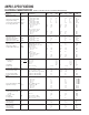
Parameter Symbol Conditions Min Typ Max Min Typ Max Unit
POWER SUPPLY
Supply Voltage Range V
S
±4.5 ±18 ±4.5 ±18 V
Supply Current I
SY
T
A
= 25°C5656mA
–40°C ≤ T
A
≤ +85°C5656mA
NOTES
1
Input voltage range guaranteed by common-mode rejection test.
2
Guaranteed by design.
3
Gain tempco does not include the effects of external component drift.
Specifications subject to change without notice.
ABSOLUTE MAXIMUM RATINGS
1, 2
Supply Voltage ±18 V
Common-Mode Input Voltage [(V–) – 60 V] to [(V+) + 60 V]
Differential Input Voltage [(V–) – 60 V] to [(V+) + 60 V]
Output Short-Circuit Duration Continuous
Operating Temperature Range –40°C to +85°C
Storage Temperature Range –65°C to +150°C
Function Temperature Range –65°C to +150°C
Lead Temperature (Soldering, 10 sec) 300°C
Package Type
JA
3
JC
Unit
8-Lead Plastic DIP (P) 96 37 °C/W
16-Lead SOIC (S) 92 27 °C/W
–IN +IN
R
G1
R
G2
25k⍀
25k⍀
25k⍀
25k⍀
V+
SENSE
OUT
REFERENCE
V–
Figure 2. Simplified Schematic
ORDERING GUIDE
V
IOS
max @ V
OOS
max @ Temperature Package
Model T
A
= 25ⴗCT
A
= 25ⴗC Range Description
AMP02EP 100 µV4 mV –40°C to +85°C 8-Lead Plastic DIP
AMP02FP 200 µV8 mV –40°C to +85°C 8-Lead Plastic DIP
AMP02AZ/883C 200 µV 10 mV –55°C to +125°C 8-Lead CERDIP
AMP02FS 200 µV8 mV –40°C to +85°C 16-Lead SOIC
AMP02GBC Die
AMP02FS-REEL 200 µV8 mV –40°C to +85°C 16-Lead SOIC
NOTES
1
Stresses above those listed under Absolute Maximum Ratings may cause perma-
nent damage to the device. This is a stress rating only; functional operation of the
device at these or any other conditions above those listed in the operational sections
of this specifications is not implied. Exposure to absolute maximum rating
conditions for extended periods may affect device reliability.
2
Absolute maximum ratings apply to both DICE and packaged parts, unless
otherwise noted.
3
θ
JA
is specified for worst case mounting conditions, i.e., θ
JA
is specified for
device in socket for P-DIP package; θ
JA
is specified for device soldered to
printed circuit board for SOIC package.